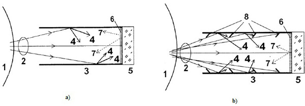
Fig. (21)
(a) Scheme of contaminating deposit appearance on the diagnostic channel “bottom” (i.e., on the optical window or the mirror). 1 – peripheral plasma; 2 – CXA flux; 3 – diagnostic channel; 4 – approximate trajectories of sputtered atoms of the diagnostic channel material (or a channel wall deposit); 5 – diagnostic window or mirror; 6 – deposit on the mirror; 7 – approximate trajectories of sputtered mirror deposit atoms. (b) Scheme of how the deposit thickness growth rate can be reduced. The notation 1 to 7 is the same as that for Fig. (22a) 8 – diaphragm from a material with a low sputtering coefficient (e.g., tungsten).