- Home
- About Journals
-
Information for Authors/ReviewersEditorial Policies
Publication Fee
Publication Cycle - Process Flowchart
Online Manuscript Submission and Tracking System
Publishing Ethics and Rectitude
Authorship
Author Benefits
Reviewer Guidelines
Guest Editor Guidelines
Peer Review Workflow
Quick Track Option
Copyediting Services
Bentham Open Membership
Bentham Open Advisory Board
Archiving Policies
Fabricating and Stating False Information
Post Publication Discussions and Corrections
Editorial Management
Advertise With Us
Funding Agencies
Rate List
Kudos
General FAQs
Special Fee Waivers and Discounts
- Contact
- Help
- About Us
- Search


The Open Materials Science Journal
(Discontinued)
ISSN: 1874-088X ― Volume 13, 2019
PL Intensity and Life-Time Enhancements of the n-GaN Light-Emitting Diode During the Device Fabrication
Shen-Li Chen1, *, Chin-Chai Chen1, Yeong-Lin Lai2, Wen-Jung Chiang2, Hung-Wei Chen1
Abstract
In this study, a thermal annealing process was used for evaluating the recovering effect of the surface bombardment in the plasma etching process. After inductively coupled plasma (ICP) etching, the n-GaN samples were heated and annealed in an N2 ambient, which influenced the electrical and photonic characteristics of the devices under test. Eventually, it showed that the resistance improved after the annealing treatment, particularly at a temperature of 550 °C. Furthermore, photoluminescence (and emission-intensity degradation) measurements yielded the same results for these n-GaN LED samples, which increased to 200% (8%) of that of a nonannealing reference group at this annealing temperature. However, this annealing treatment did not completely repair the luminescence intensity and emission life-time because of the formation of deep-level point defects on the n-GaN sample surface during the fabrication process.
Article Information

Identifiers and Pagination:
Year: 2016Volume: 10
Issue: Suppl-1, M2
First Page: 20
Last Page: 28
Publisher Id: TOMSJ-10-20
DOI: 10.2174/1874088X01610010020
Article History:
Received Date: 8/4/2015Revision Received Date: 15/5/2015
Acceptance Date: 4/7/2015
Electronic publication date: 15/07/2016
Collection year: 2016
open-access license: This is an open access article licensed under the terms of the Creative Commons Attribution-Non-Commercial 4.0 International Public License (CC BY-NC 4.0) (https://creativecommons.org/licenses/by-nc/4.0/legalcode), which permits unrestricted, non-commercial use, distribution and reproduction in any medium, provided the work is properly cited.
* Address correspondence to this author at the Department of Electronic Engineering, National United University, MiaoLi City 36063, Taiwan; Tel: +886-37-382525; Fax: +886-37-362498; E-mail: jackchen@nuu.edu.tw
| Open Peer Review Details | |||
|---|---|---|---|
| Manuscript submitted on 8-4-2015 |
Original Manuscript | PL Intensity and Life-Time Enhancements of the n-GaN Light-Emitting Diode During the Device Fabrication | |
INTRODUCTION
III-V nitride-based materials have become major semiconductors for optoelectronic devices such as blue-light-emitting diodes (LEDs) and laser diodes (LDs). Gallium nitride (GaN) is a wide-bandgap and high-bond-energy semiconductor material. Because GaN is chemically stable and insoluble in all mineral acids [1Lee H, Oberman DB, James S. Reactive ion etching of GaN using CHF3/Ar and C2ClF5/Ar plasmas. Appl Phys Lett 1995; 67: 1754-6.
[http://dx.doi.org/10.1063/1.115039] -6Xu L, Pan G, Zou C, Shi X, Liu Y. Atomically smooth gallium nitride surfaces generated bychemical mechanical polishing with non-noble metal catalyst(Fe-Nx/C) in acid solution. In: International Conference on Planarization/CMP Technology (ICPT). 2014; pp. 237-41.], performing wet etching during device fabrication is extremely difficult. Therefore, for fabricating blue LEDs or LDs, we used dry etching techniques such as reactive-ion-etching (RIE), inductively coupled plasma (ICP), and electron cyclotron resonance (ECR) reactors. However, bombardment of energetic ions damages the surface critical layer of a GaN device. Heavy ion bombardment of the crystal surface at low pressure produces pits, craters, and hillocks [7Kucheyev SO, Williams JS, Jagadish C, Li G, Pearton SJ. Strong surface disorder and loss of N produced by ion bombardment of GaN. Appl Phys Lett 2000; 76: 3899-901.
[http://dx.doi.org/10.1063/1.126814] -14Velasco AJ, Chacon AL, Serrano WA. Negative ion generation and isotopic effect in electron cyclotron resonance plasma. IEEE Trans Plasma Sci 2015; 1-4.]. The formation of these defects is explained by variations in the sputtering rate across the surface because of irregularities and defects in the surface. We classified these damage defects according to the lattice disorders and point defects.
The layer distribution of a completely formatted structure of GaN-based blue LED is shown in Fig. (1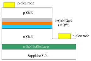 ). The epitaxial structure of a GaN-based LED from bottom to top is sequentially presented as follows. An undoped u-GaN buffer layer and u-GaN layer were grown on a sapphire substrate to facilitate the growth of the single crystal material n-GaN. The n-AlGaN and InGaN/GaN multiquantum well (MQW) active layers and the p-AlGaN and p-GaN layers were then grown on the single crystal n-GaN. The MQW active layer, composed of InGaN/GaN, is the primary area that irradiated blue light when a forward-bias voltage was applied between the two electrodes.
Electron-hole recombination occurred at the P/N junction, and released photon energy, which was radiated in a photonic emission. ICP etching was employed to etch back the n-GaN electrode area after the various layers were grown, and coat a transparent conductive layer (TCL). The TCL uniformly spread currents, preventing conduction crowding. Finally, the p- and n-electrode areas of this LED were coated with gold (Au) for wiring and creating contacts. In this study, we used Cl2/Ar gas sources to etch the n-GaN surface in an ICP system. The plasma reactor is shown in Fig. (2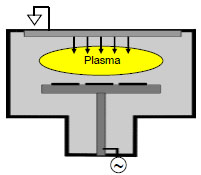 ). The main reason for using the Cl2-based plasma was to form GaCl3 and NCl3 [15Gao Z, Romero MF, Calle F. Etching of AIGaN/GaN HEMT structures by Cl2-based ICP. In: Spanish Conference on Electron Devices. 2013; pp. 29-32.]. The surface was expected to be Ga-rich because of the high volatility of the NCl3. The addition of an Ar source should efficiently remove etching residue products on the surface. However, attention should be focused on the induced damage problem on the GaN surface. Therefore, a thermal-annealing treatment was used for preventing surface damage on the n-GaN material after the dry etching process.
 |
Fig. (1) Cross-section view of a preliminary formation structure of GaN blue LED. |
 |
Fig. (2) Schematic illustration of an inductively-coupled-plasma reactor. |
EXPERIMENTAL DETAILS ABOUT THE N-GAN PROCESS
The assistance of dc bias voltage is a major factor in the ICP process [16Kim H, Schuette ML, Lu WCl. 2/BCl3/Ar plasma etching and in situ oxygen plasma treatment for leakage current suppression in AlGaN/GaN high-electron mobility transistors. J Vac Sci Technol B 2011; 29: 031204-5. [Microelectron Nanometer Struct].
[http://dx.doi.org/10.1116/1.3581090] ]. The variation of dc bias achieved by changing the coil and platen power in a Cl2/Ar plasma system is shown in Fig. (3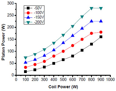 ). In general, to increase the dc bias voltage, more energetic ions must be bombarded. Preliminarily, the n-GaN samples used in this study were grown on a sapphire substrate through metal-organic chemical vapor deposition and were approximately 3.5 μm thick. This n-type GaN layer had a carrier concentration of approximately 3 × 1018 cm−3. In the following experimental groups, the device-under-test (DUT) samples were etched using an ICP process by using Cl2/Ar gas sources in an STS plasma system. A total gas flow rate of 50 sccm and etching duration time of 60 s was chosen as the optimal condition (Fig. 3). In addition, all samples were etched using a platen power of 120 W and a dc bias voltage of −100 V. Table 1 lists the detailed physical parameters of the fabrication process.
For easy implementation, a dry etching process was required for fabricating GaN electronic devices. To improve and recover the electric properties caused by ion-induced damage, the n-GaN samples were treated using a thermal-annealing process in an N2 ambient after dry etching. In this study, annealing was performed in a flowing N2 gas atmosphere for 40 min and as a function of ambient temperatures (500, 550, and 600 °C). After the annealing, some of the DUTs of the n-GaN materials were deposited on the Ti/Al metal layer through e-beam evaporation and were lifted-off, then alloyed at 550 °C for 5 min to form satisfactory ohmic contact; however, the remaining DUTs of the complete LED devices were fabricated as described in Section 1 (Introduction).
 |
Fig. (3) Platen power vs. coil power in an ICP system as the DC-bias voltage (negative value) varied. |

MEASUREMENT RESULTS AND DISCUSSION
PL Intensity Measurement in the n-GaN Material DUTs
As a benchmark, a reference DUT was not subjected to annealing. The I-V measurement data of an n-GaN material were tested using a semiconductor parameter analyzer. Fig. (4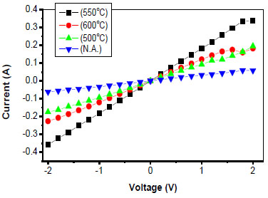 ) shows a comparison of I-V characteristics after N2 annealing treatments under thermal temperatures of 500, 550, and 600 °C and the reference DUT. A significant increase occurred in the I-V slope at 550-600 °C because of defects, which can be repaired by thermal energy. Therefore, resistance after the dry etching process decreased because of exposure at 550 °C for 40 min. This decreasing contact-resistance characteristic is crucial for the improvement of the forward voltage in LED production.
 |
Fig. (4) Comparisons of I-V measurement data after three different N2 annealing treatments (40 min.) and a reference DUT (none with any thermal annealing). |
Furthermore, defects were induced by the energetic ion bombardment in the ICP etching system during n-GaN material fabrication, which included numerous point and structural defects. These defects considerably affected the electrical and optical properties of the host material and severely reduced the performance and reliability of the devices created on the basis of III-V nitride-based semiconductors. Therefore, PL is always used for detecting defects in semiconductor materials [17Reshchikov MA, Morkoc H. Luminescence properties of defects in GaN. J Appl Phys 2005; 97: 061301-95.
[http://dx.doi.org/10.1063/1.1868059] -22Tajima M. Spectroscopy and topography of deep-level luminescence in photovoltaic silicon. IEEE J Photovolt 2014; 4(6): 1452-8.
[http://dx.doi.org/10.1109/JPHOTOV.2014.2350082] ]. Fig. (5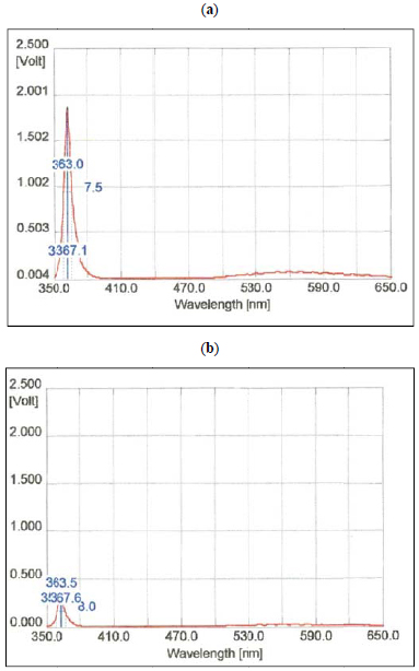 ) shows a comparison of PL spectrum intensity before and after the ICP dry etching process, in which the downgrade percentage reached about 84.14%. Figs. (6
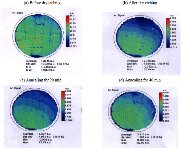 -8
-8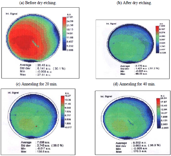 ) show the comparisons of luminescence intensity mapping (2" wafer) at an annealing temperature of 500, 550, and 600 °C at 0, 20, and 40 min, respectively. The luminescence intensities decreased dramatically after the dry etching process for wafer-1~ wafer 3 are shown in Fig. (9
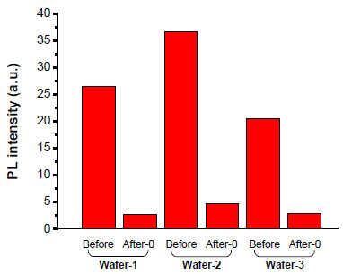 ). Typically, when a sample is annealed in a furnace (550 °C) for 40 min, the average luminescence intensity increases from 4.697 to 14.33 (au). The luminescence intensity before and after the annealing treatment indicated that the annealing treatment effectively repaired some of the dry-etching-induced damage. Fig. (10
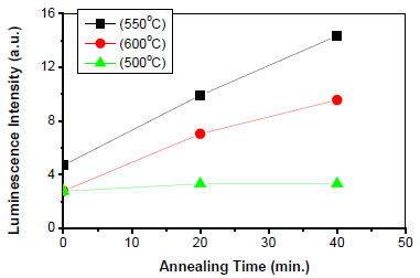 ) shows the average luminescence intensity increase with annealing time, typically at 550 °C, where a satisfactory consistency in I-V measurements was also obtained in Fig. (4).
 |
Fig. (5) Comparisons of PL spectrum intensity (a) before and (b) after ICP dry etching process. |
 |
Fig. (6) PL intensity mappings vs. thermal-annealing time under the 500 °C situation. |
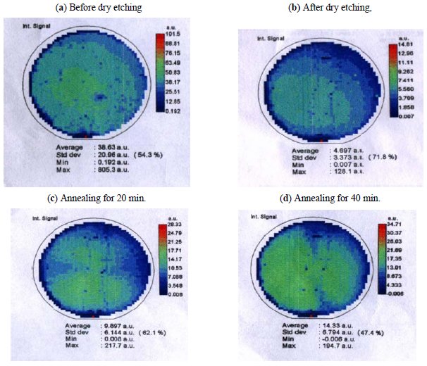 |
Fig. (7) PL intensity mappings vs. thermal-annealing time under the 550 °C situation. |
 |
Fig. (8) PL intensity mappings vs. thermal-annealing time under the 600 °C situation. |
 |
Fig. (9) Average PL intensities before and just after ICP dry etching for the wafer-1~ wafer-3. |
Emission Life-Test: Degradation Suspension in the GaN LEDs
When a plasma etching process was proceeded for GaN LED device fabrication, a dc bias voltage of −110 V was applied. After this etching process, some surface damages caused by the etching ion bombardment still existed. Therefore, at 550 °C thermal annealing (activation process) was implemented for 40 min during the manufacture of the blue LEDs to observe the effect on the emission live test performance. In thermal annealing, the same wafer was divided into two testing groups; the first group underwent the thermal annealing activation, whereas the other did not. However, to avoid confusion, the DUT of these two groups followed the same aforementioned procedure. Fig. (11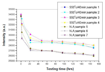 ) shows GaN LED devices continuously lightened using 20 mA electric current at room temperature for 168 h (testing time). Obviously, for nonactivation processing devices such as Samples 5~7, the corresponding emission light intensity decay reached 26.3%, but for the thermal annealing activated devices, the emission light decay decreased by only 18.2%. Continuous lighting by electrical current flow excited the spontaneous decay phenomenon, which was unavoidable. However, in the long-term performance measurement of these GaN devices, GaN emission life-time property may be improved using a suitable thermal annealing treatment.
 |
Fig. (10) A comparison of average PL intensity vs. thermal-annealing times. |
 |
Fig. (11) Comparisons of light-intensity degradation during life-time testing as for the thermal-annealing treatment and non-activated (reference) DUTs. |
CONCLUSION
The defects on the surface of n-GaN materials and GaN LEDs caused by plasma dry etching by using an ICP reactor were investigated in this study. We demonstrated the thermal annealing influence on the emission characteristic of the n-GaN materials and GaN devices. Furthermore, a suitable thermal annealing treatment of the GaN samples might improve the luminescence intensity and emission life time. From the experimental data, the resistance decreased dramatically because of exposure at 550 ˚C for 40 min of annealing in an N2 ambient after dry etching. In addition, the luminescence intensity and emission life time were improved in most aspects typically at 550 ˚C annealing temperature, which was because of the improvement of crystal quality at the surface and reduction of nonradioactive related centers (called recombination centers) in the material.
CONFLICT OF INTEREST
The authors confirm that this article content has no conflict of interest.
ACKNOWLEDGEMENTS
Declared none.
REFERENCES
| [1] | Lee H, Oberman DB, James S. Reactive ion etching of GaN using CHF3/Ar and C2ClF5/Ar plasmas. Appl Phys Lett 1995; 67: 1754-6. [http://dx.doi.org/10.1063/1.115039] |
| [2] | Haberer ED, Chen CH, Hansen M, et al. Enhanced diffusion as a mechanism for ion-induced damage propagation in GaN. J Vac Sci Technol B 2001; 19: 603-8. [Microelectron Nanometer Struct]. [http://dx.doi.org/10.1116/1.1362684] |
| [3] | Abidin MS, Sharifabad ME, Hashim AM, Rahman SF, Rahman AR, Osman MN. Fabrication of open gate structure on GaN-based HEMT for pH sensing. In: International Semiconductor Device Research Symposium (ISDRS). 2009; pp. 1-2. [http://dx.doi.org/10.1109/ISDRS.2009.5378191] |
| [4] | Lee C, Hite JK, Mastro MA, et al. Selective chemical etch of gallium nitride by phosphoric acid. J Vac Sci Technol A 2012; 30: 040602-3. [Vac Surfaces Films]. [http://dx.doi.org/10.1116/1.4719528] |
| [5] | Zhang Y, Guo E, Li Z, et al. Light extraction efficiency improvement by curved GaN sidewalls in InGaN-Based light-emitting diodes. IEEE Photonics Technol Lett 2012; 24: 243-5. [http://dx.doi.org/10.1109/LPT.2011.2177251] |
| [6] | Xu L, Pan G, Zou C, Shi X, Liu Y. Atomically smooth gallium nitride surfaces generated bychemical mechanical polishing with non-noble metal catalyst(Fe-Nx/C) in acid solution. In: International Conference on Planarization/CMP Technology (ICPT). 2014; pp. 237-41. |
| [7] | Kucheyev SO, Williams JS, Jagadish C, Li G, Pearton SJ. Strong surface disorder and loss of N produced by ion bombardment of GaN. Appl Phys Lett 2000; 76: 3899-901. [http://dx.doi.org/10.1063/1.126814] |
| [8] | Kucheyev SO, Williams JS, Zou J, Jagadish C, Li G. Disordering and anomalous surface erosion of GaN during ion bombardment at elevated temperatures. Appl Phys Lett 2001; 78: 1373-5. [http://dx.doi.org/10.1063/1.1347010] |
| [9] | Petravic M, Coleman VA, Kim KJ, Li G. Defect acceptor and donor in ion-bombarded GaN. J Vac Sci Technol A 2005; 23: 1340-5. [Vac Surfaces Films]. [http://dx.doi.org/10.1116/1.1991869] |
| [10] | Davies RP, Gila BP, Abernathy CR, Pearton SJ, Stanton CJ. Defect-enhanced ferromagnetism in Gd- and Si co-implanted GaN. Appl Phys Lett 2010; 96: 212502-212502-3. [http://dx.doi.org/10.1063/1.3437085] |
| [11] | Emilie DP, Chabert P. MD simulations of GaN sputtering by Ar+ ions: Ion-induced damage and near-surface modification under continuous bombardment. J Vac Sci Technol A 2010; 28: 1105-10. [Vac Surfaces Films]. [http://dx.doi.org/10.1116/1.3460904] |
| [12] | Peter R, Segota D, Petravic M. Point defects in gallium nitride: X-ray absorption measurements and multiple scattering simulations. Appl Phys Lett 2011; 99: 172107-172107-3. [http://dx.doi.org/10.1063/1.3656701] |
| [13] | Afanas'ev VV, Nguyen AP, Houssa M, Stesmans A, Tokei Z, Baklanov MR. High-resolution electron spin resonance analysis of ion bombardment induced defects in advanced low-κ insulators (κ = 2.0-2.5). Appl Phys Lett 2013; 102: 172908-4. [http://dx.doi.org/10.1063/1.4801938] |
| [14] | Velasco AJ, Chacon AL, Serrano WA. Negative ion generation and isotopic effect in electron cyclotron resonance plasma. IEEE Trans Plasma Sci 2015; 1-4. |
| [15] | Gao Z, Romero MF, Calle F. Etching of AIGaN/GaN HEMT structures by Cl2-based ICP. In: Spanish Conference on Electron Devices. 2013; pp. 29-32. |
| [16] | Kim H, Schuette ML, Lu WCl. 2/BCl3/Ar plasma etching and in situ oxygen plasma treatment for leakage current suppression in AlGaN/GaN high-electron mobility transistors. J Vac Sci Technol B 2011; 29: 031204-5. [Microelectron Nanometer Struct]. [http://dx.doi.org/10.1116/1.3581090] |
| [17] | Reshchikov MA, Morkoc H. Luminescence properties of defects in GaN. J Appl Phys 2005; 97: 061301-95. [http://dx.doi.org/10.1063/1.1868059] |
| [18] | Yoshikawa M, Sugie R, Murakami M, Matsunobe T, Matsuda K, Ishida H. Defect characterization of Si-doped GaN films by a scanning near-field optical microscope-induced photoluminescence. Appl Phys Lett 2006; 88: 161905-3. [http://dx.doi.org/10.1063/1.2190270] |
| [19] | Kubota M, Onuma T, Ishihara Y, Usui A, Uedono A, Chichibu SF. Thermal stability of semi-insulating property of Fe-doped GaN bulk films studied by photoluminescence and mono energetic positron annihilation techniques. J Appl Phys 2009; 105: 083542-9. [http://dx.doi.org/10.1063/1.3110205] |
| [20] | Izyumskaya N, Zhang F, Okur S, et al. Optical studies of strain and defect distribution in semipolar (1101) GaN on patterned Si substrates. J Appl Phys 2013; 114: 113502-9. [http://dx.doi.org/10.1063/1.4821343] |
| [21] | Johnston S, Guthrey H, Yan F, et al. Correlating multicrystalline silicon defect types using photoluminescence, defect-band emission, and lock-in thermography imaging techniques. IEEE J Photovolt 2014; 4(1): 348-54. [http://dx.doi.org/10.1109/JPHOTOV.2013.2283575] |
| [22] | Tajima M. Spectroscopy and topography of deep-level luminescence in photovoltaic silicon. IEEE J Photovolt 2014; 4(6): 1452-8. [http://dx.doi.org/10.1109/JPHOTOV.2014.2350082] |