- Home
- About Journals
-
Information for Authors/ReviewersEditorial Policies
Publication Fee
Publication Cycle - Process Flowchart
Online Manuscript Submission and Tracking System
Publishing Ethics and Rectitude
Authorship
Author Benefits
Reviewer Guidelines
Guest Editor Guidelines
Peer Review Workflow
Quick Track Option
Copyediting Services
Bentham Open Membership
Bentham Open Advisory Board
Archiving Policies
Fabricating and Stating False Information
Post Publication Discussions and Corrections
Editorial Management
Advertise With Us
Funding Agencies
Rate List
Kudos
General FAQs
Special Fee Waivers and Discounts
- Contact
- Help
- About Us
- Search


The Open Materials Science Journal
(Discontinued)
ISSN: 1874-088X ― Volume 13, 2019
Characteristics of GaAs Power MESFETs with Double Silicon Ion Implantations for Wireless Communication Applications
Chun-Yi Zheng1, Wen-Jung Chiang1, Yeong-Lin Lai*, 2, Edward Y. Chang3, Shen-Li Chen4, K. B. Wang3
Abstract
GaAs power metal-semiconductor field-effect transistors (MESFETs) were fabricated using direct double silicon (Si) ion implantation technology for wireless communication applications. A 150-µm MESFET had a saturation drain current of 238 mA/mm after Si3N4 passivation. A 15-mm MESFET, when measured under a class-AB condition with a biased drain voltage of 3.4 V and a quiescent drain current of 600 mA, delivered a maximum output power (Pout) of 31.1 dBm and a maximum power-added efficiency (PAE) of 58.0% at a frequency of 1.88 GHz. The MESFET exhibited a Pout of 29.2 dBm with a PAE of 45.0% at the 1-dB gain compression point. The MESFET, when measured under a deep class-B condition with a biased drain voltage of 4.7 V and a quiescent drain current of 50 mA, achieved a maximum Pout of 33.1 dBm and a maximum PAE of 55.9% at 1.88 GHz. The MESFET operating at 4.7 V and 1.88 GHz exhibited a P1dB of 31.8 dBm and an associated PAE of 47.1% at the 1-dB gain compression point. When tested by IS-95 code-division multiple access (CDMA) standard signals and biased at 4.7 V under the deep class-B condition, the MESFET with a Pout of 28 dBm demonstrated an adjacent channel power rejection (ACPR) of –31.2 dBc at +1.25 MHz apart from the 1.88 GHz center frequency and –45.7 dBc at +2.25 MHz.
Article Information

Identifiers and Pagination:
Year: 2016Volume: 10
Issue: Suppl-1, M3
First Page: 29
Last Page: 36
Publisher Id: TOMSJ-10-29
DOI: 10.2174/1874088X01610010029
Article History:
Received Date: 10/4/2015Revision Received Date: 15/5/2015
Acceptance Date: 12/7/2015
Electronic publication date: 15/06/2016
Collection year: 2016
open-access license: This is an open access article licensed under the terms of the Creative Commons Attribution-Non-Commercial 4.0 International Public License (CC BY-NC 4.0) (https://creativecommons.org/licenses/by-nc/4.0/legalcode), which permits unrestricted, non-commercial use, distribution and reproduction in any medium, provided the work is properly cited.
* Address correspondence to this author at the Department of Mechatronics Engineering, National Changhua University of Education, Changhua 50007, Taiwan; Tel: +886-4-7232105; Fax: +886-4-7211149; E-mail: yllai@cc.ncue.edu.tw
| Open Peer Review Details | |||
|---|---|---|---|
| Manuscript submitted on 10-4-2015 |
Original Manuscript | Characteristics of GaAs Power MESFETs with Double Silicon Ion Implantations for Wireless Communication Applications | |
INTRODUCTION
Power transistors are key components of the power amplifiers in the transmitters of wireless communication systems [1Lai Y-L, Chang EY, Chang CY, et al. 5mm high-power-density dual-delta-doped power HEMT’s for 3 V L-band applications. IEEE Electron Device Lett 1996; 17(5): 229-31.
[http://dx.doi.org/10.1109/55.491838] -14Chang EY, Lai Y-L, Lee YS, Chen SH. GaAs/AlAs wet selective etch process for the gate recess of GaAs power metal-semiconductor field-effect transistors. J Electrochem Soc 2001; 148(1): G4-9.
[http://dx.doi.org/10.1149/1.1344555] ]. There is a great demand for high-performance power transistors which meet the requirements of advanced wireless communication systems [15Kim J, Kim D, Cho Y, et al. Supply modulator for envelope-tracking operation of dual-mode handset power amplifier In: Proceedings of European Microwave Conference (EuMC); 6-10 Oct 2013; Nuremberg, Germany; 2013; pp 1315-8. Available from: http://ieeexplore.ieee.org/xpl/login.jsp?tp=&arnumber=6686907&url=http%3A%2F%2Fieeexplore.ieee.org%2Fxpls%2Fabs_all.jsp%3Farnumber%3D6686907-23Choi P, Goswami S, Radhakrishna U, et al. A 5.9-GHz fully integrated GaN frontend design with physics-based RF compact model. IEEE Trans Microw Theory Tech 2015; 63(4): 1163-73.
[http://dx.doi.org/10.1109/TMTT.2015.2405913] ]. Ion-implanted GaAs power metal-semiconductor field-effect transistors (MESFETs) have been studied as to their wireless communication applications [24Maeda M, Nishijima M, Takehara H, et al. A 3.5V, 1.3W GaAs power multichip IC for cellular phone. In: Proceedings of IEEE GaAs IC
Symposium Digest; 10-13 Oct. 1993; San Jose, California, USA; 1993; pp. 53-6.
[http://dx.doi.org/10.1109/GAAS.1993.394501] -29Chang EY, Fuh C-S, Meng CC, Wang KB, Chen SH. A planar gate double beryllium implanted GaAs power MESFET for low voltage digital wireless communication application. IEEE Trans Electron Dev 2000; 47(6): 1134-8.
[http://dx.doi.org/10.1109/16.842954] ]. A GaAs power multi-chip integrated circuit using ion-implanted GaAs power MESFETs delivered an output power (Pout) of 1.3 W at 3.5 V for cellular phone communications from 890 to 950 MHz [24Maeda M, Nishijima M, Takehara H, et al. A 3.5V, 1.3W GaAs power multichip IC for cellular phone. In: Proceedings of IEEE GaAs IC
Symposium Digest; 10-13 Oct. 1993; San Jose, California, USA; 1993; pp. 53-6.
[http://dx.doi.org/10.1109/GAAS.1993.394501] ]. High-efficiency GaAs power MESFETs with an asymmetrical lightly-doped drain structure gave 32.5-dB output power at 4.7 V for 950-MHz communications [25Yanagihara M, Ota Y, Nishii K, Ishikawa O, Tamura A. Highly efficient GaAs power MESFETs with n+-asymmetrical LDD structure. Electron Lett 1992; 28(7): 686-7.
[http://dx.doi.org/10.1049/el:19920433] ]. Conventional ion-implanted GaAs power MESFETs were developed for analog communication applications. Instead of analog wireless communications, digital wireless communications have dominated the wireless trend because of their higher capacity. An analog/digital dual-mode power module with ion-implanted GaAs power MESFETs showed a power-added efficiency (PAE) of 56% at 3.7 V for the North American digital cellular (NADC) communications [26Masato H, Maeda M, Fujimoto H, et al. Analogue/digital dual power module using ion-implanted GaAs MESFETs. In: Proceedings of IEEE
MTT-S International Microwave Symposium Digest; 16-20 May 1995; Orlando, Florida, USA; 1995; 2: pp. 567-70.
[http://dx.doi.org/10.1109/MWSYM.1995.406023] ]. A 36-mm GaAs power MESFET using selective ion implantation and semi-insulating setback layer technologies delivered a Pout of 31.5 dBm at 5.8 V for digital communication applications [27Furukawa H, Tateoka K, Miyatsuji K, Sugimura A, Ueda D. A novel GaAs power MESFET with low distortion characteristics employing semi-insulating setback layer under the gate. IEEE Trans Electron Dev 1996; 43(2): 193-200.
[http://dx.doi.org/10.1109/16.481717] ]. Most ion-implanted GaAs power MESFETs have been implemented by means of selective ion implantation technology [24Maeda M, Nishijima M, Takehara H, et al. A 3.5V, 1.3W GaAs power multichip IC for cellular phone. In: Proceedings of IEEE GaAs IC
Symposium Digest; 10-13 Oct. 1993; San Jose, California, USA; 1993; pp. 53-6.
[http://dx.doi.org/10.1109/GAAS.1993.394501] -27Furukawa H, Tateoka K, Miyatsuji K, Sugimura A, Ueda D. A novel GaAs power MESFET with low distortion characteristics employing semi-insulating setback layer under the gate. IEEE Trans Electron Dev 1996; 43(2): 193-200.
[http://dx.doi.org/10.1109/16.481717] ]. The alignment and process of the n+ source and drain selectively-implanted regions are critical for the characteristics of MESFETs. Lai and coworkers first reported on GaAs power MESFETs using direct ion implantation technology, with silicon (Si) and beryllium (Be) ion implantations, for low-voltage digital wireless communication applications [28Lai Y-L, Chang EY, Chang C-Y, et al. High-efficiency and low-distortion directly-ion-implanted GaAs power MESFET’s for digital personal handy-phone applications. IEEE Electron Dev Lett 1997; 18(9): 429-31.
[http://dx.doi.org/10.1109/55.622519] ]. A 2.2-V-operation GaAs power MESFET with a gate width of 2 mm demonstrated an adjacent channel power rejection (ACPR) of –58 dBc and a PAE of 57.2% at a Pout of 21.3 dBm. A planar-gate GaAs power MESFET with direct Si and Be ion implantations also showed good characteristics at 3.6 V [29Chang EY, Fuh C-S, Meng CC, Wang KB, Chen SH. A planar gate double beryllium implanted GaAs power MESFET for low voltage digital wireless communication application. IEEE Trans Electron Dev 2000; 47(6): 1134-8.
[http://dx.doi.org/10.1109/16.842954] ]. GaAs power MESFETs with direct ion implantations provide a cost-effective solution for digital wireless communications [30Feng M, Shen S-C, Caruth DC, Huang J-J. Device technologies for RF front-end circuits in next-generation wireless communications. Proc IEEE 2004; 92(2): 354-75.
[http://dx.doi.org/10.1109/JPROC.2003.821903] ].
In this study, GaAs power MESFETs were fabricated by means of direct double Si ion implantations for digital wireless communication applications. The power characteristics of the MESFETs including Pout, PAE, gain, and ACPR were demonstrated.
FABRICATION
The GaAs power MESFETs were fabricated with double 29Si+-ion implantations into a semi-insulating GaAs wafer. Channel implantation was conducted by 29Si+ ion implantation with an energy of 200 keV and a dosage of 3.0 × 1012 cm-2 to form a channel layer with high current capability. Surface implantation was implemented by 29Si+ ion implantation with an energy of 50 keV and a dosage of 1.0 × 1012 cm-2 to form a low-resistivity ohmic layer.
The GaAs wafer was sputtered with silicon nitride film for the passivation process after double 29Si+-ion implantations. The passivation process was used to prevent the decomposition of the GaAs material and the loss of arsenic atoms during the subsequent activation process with high-temperature annealing. The activation process was carried out by rapid thermal annealing (RTA) at 800°C. The sheet resistance of wafer after annealing was 512 Ω/□.
The Au/Ge/Ni/Au ohmic metal with a thickness of 0.4 μm was deposited by an electron gun system and alloyed by RTA at 330°C. The specific contact resistance of the ohmic contact was in the 10-7-Ω∙cm2 range. The Ti/Pt/Au gate metal with a gate length of 1 μm was formed after a gate recess process. The gate widths of the MESFETs included 150 μm and 15 mm. A silicon nitride passivation layer was deposited using a plasma-enhanced chemical vapor deposition (PECVD) system in order to protect the device from humidity and contamination. The fabricated power MESFET with a gate width of 15 mm is shown in Fig. (1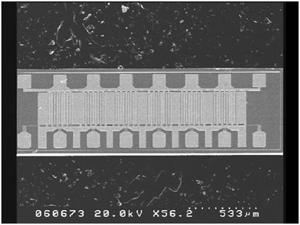 ). Once the front-side process was completed, the backside of the wafer was lapped to 4 mils and plated by gold metal in order to improve the thermal conductance.
 |
Fig. (1) Fabricated GaAs power MESFET with a gate width of 15 mm. |
PERFORMANCE
The on-wafer measurements of the DC characteristics of the MESFETs, including the current-voltage and breakdown characteristics, were conducted in order to monitor and control the processes during the fabrication of the MESFETs. A MESFET with a gate width of 150 μm, rather than 15 mm, was used for the on-wafer DC measurement, because devices with a small gate width would not generate a current large enough to damage themselves. Fig. (2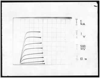 ) shows the current-voltage characteristics of the MESFET with a gate width of 150 µm after the Si3N4 passivation. The saturation drain current of the device was 35.7 mA, corresponding to a current density of 238 mA/mm. Fig. (3
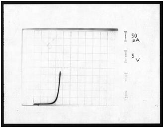 ) shows the gate-to-drain breakdown characteristics after the Si3N4 passivation. The gate-to-drain breakdown voltage was 17 V. The current-voltage characteristics of the 150-μm MESFET after the airbridge process are shown in Fig. (4
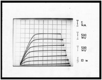 ). The saturation drain current of the MESFET was 35 mA, corresponding to a current density of 233 mA/mm. The saturation drain current characteristics after the Si3N4 passivation and airbridge processes were very close.
 |
Fig. (2) Current-voltage characteristics of 150-µm MESFET after Si3N4 passivation. |
 |
Fig. (3) Gate-to-drain breakdown characteristics after Si3N4 passivation. |
The gate-to-drain breakdown characteristics after the airbridge process are shown in Fig. (5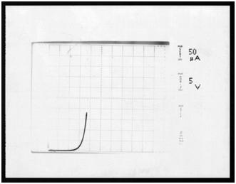 ). The gate-to-drain breakdown voltage was 17 V. The gate-to-drain breakdown characteristics after the Si3N4 passivation and airbridge processes were the same.
 |
Fig. (4) Current-voltage characteristics of 150-µm MESFET after airbridge process. |
The power characteristics of the MESFET with a gate width of 15 mm were measured by means of a load-pull power tuning system. The impedances of the input and output tuners of the system were tuned to obtain the optimum source and load matching for maximum Pout and PAE. The measurement frequency was 1.88 GHz. The MESFET was biased at operation voltages of 3.4 V and 4.7 V. When the MESFET was biased at a drain voltage of 3.4 V, it was tested under a class-AB condition with a quiescent drain current of 600 mA.
When the MESFET was biased at a drain voltage of 4.7 V, it was expected that it would have better power performance than the one biased at 3.4 V because of the higher voltage supply. A more stringent condition, a deep class-B condition with a quiescent drain current of 50 mA, was adopted at 4.7 V in order to evaluate the extreme power capability of the MESFET as far as the linearity was concerned.
 |
Fig. (5) Gate-to-drain breakdown characteristics after airbridge process. |
Fig. (6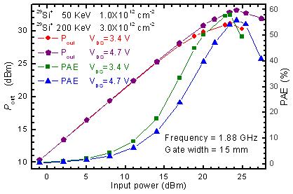 ) depicts the Pout and PAE as functions of the input power for the MESFET biased at 3.4 V and 4.7 V. The device operating at 3.4 V demonstrated a maximum Pout of 31.1 dBm and a maximum PAE of 58.0%. The Pout at the 1-dB gain compression point (P1dB) and the associated PAE were 29.2 dBm and 45.0%, respectively. The MESFET operating at a drain voltage of 4.7 V achieved a maximum Pout of 33.1 dBm and a maximum PAE of 55.9%. At a P1dB of 31.8 dBm, the MESFET operating at 4.7 V exhibited a PAE of 47.1%. It was found that the MESFET operating at 4.7 V displayed better maximum Pout and P1dB, even under a deep class-B condition, than one operating at 3.4 V under a class-AB condition.
 |
Fig. (6) Pout and PAE as a function of input power for 15-mm MESFET biased at 3.4 V and 4.7 V. |
Fig. (7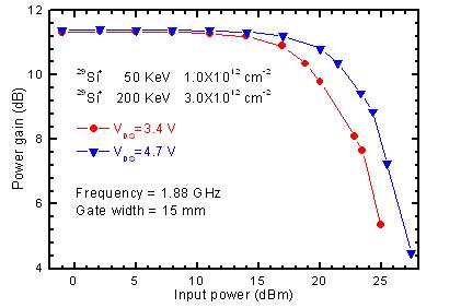 ) shows the power gain as a function of the input power for the MESFET biased at 3.4 V and 4.7 V. The linear gain characteristics of the MESFET operating at 3.4 V and 4.7 V were 11.3 dB and 11.4 dB, respectively. The linear gain characteristics of the MESFET at 3.4 V under the class-AB condition were comparable to those at 4.7 V under the deep class-B condition. The GaAs power MESFET using double ion implantation technology demonstrated high Pout and PAE. In addition, the high P1dB associated with high efficiency indicated high linearity and low distortion for digital wireless communication applications.
 |
Fig. (7) Power gain as a function of input power for 15-mm MESFET biased at 3.4 V and 4.7 V. |
The 15-mm MESFET was tested for digital wireless applications. The device was measured using modulated IS-95 code-division multiple access (CDMA) standard signals. The signal source was the Anritsu-MG3670C digital modulation signal generator. The output power spectrum of the device was measured by the HP-8595E spectrum analyzer. The data were taken when the device was biased at a drain voltage of 4.7 V under a deep class-B condition. The quiescent drain current of the device was 50 mA. Fig. (8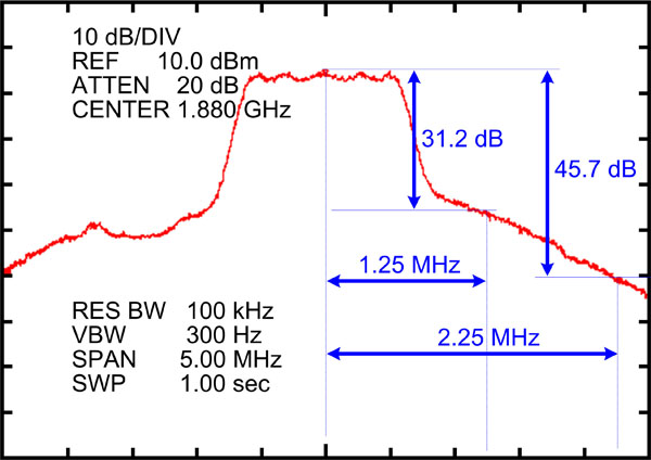 ) shows the CDMA output power spectrum of the MESFET. At a Pout of 28 dBm, the device exhibited an ACPR of –31.2 dBc at +1.25 MHz apart from the 1.88-GHz center frequency, and an ACPR of –45.7 dBc at +2.25 MHz. The power MESFET achieved excellent ACPR characteristics at an extremely low bias current for CDMA wireless communication applications.
In this study, the GaAs power MESFETs were fabricated using double 29Si+-ion implantations, including channel implantation with an implantation energy of 200 keV and an implantation dosage of 3.0 × 1012 cm-2, and surface implantation with an implantation energy of 50 keV and an implantation dosage of 1.0 × 1012 cm-2. On the basis of the study results, more implantation energy and dosage conditions can be set as parameters for further study of the characteristics of GaAs power MESFETs with respect to various modern wireless communication applications.
 |
Fig. (8) CDMA output power spectrum of 15-mm MESFET. |
CONCLUSION
The GaAs power MESFETs were fabricated by means of double Si ion implantation technology for wireless communications. The power performance of the MESFET for digital wireless communication applications was studied. The MESFET operating at 3.4 V and 1.88 GHz achieved a Pout of 31.1 dBm, a PAE of 58.0%, and a linear gain of 11.3 dB. At a deep class-B condition, the MESFET biased at 50 mA and 4.7 V exhibited an ACPR of –31.2 dBc at +1.25 MHz apart from the 1.88-GHz center frequency, while the Pout was 28 dBm. The power MESFET using direct double Si ion implantations, with the advantages of high yields and low costs, demonstrated excellent power characteristics for digital wireless communication applications.
CONFLICT OF INTEREST
The authors confirm that this article content has no conflict of interest.
ACKNOWLEDGEMENTS
This work was supported in part by the Ministry of Science and Technology of Taiwan, R.O.C. under Contracts MOST 103-2911-I-009-302, MOST 103-2221-E-018-021 and MOST 104-2221-E-018-016.
REFERENCES
| [1] | Lai Y-L, Chang EY, Chang CY, et al. 5mm high-power-density dual-delta-doped power HEMT’s for 3 V L-band applications. IEEE Electron Device Lett 1996; 17(5): 229-31. [http://dx.doi.org/10.1109/55.491838] |
| [2] | Inosako K, Matsunaga K, Okamoto Y, Kuzuhara M. Highly efficient double-doped heterojunction FET’s for battery-operated portable power applications. IEEE Electron Device Lett 1994; 15(7): 248-50. [http://dx.doi.org/10.1109/55.294085] |
| [3] | Lai Y-L, Chang EY, Lee D-H, Chen S-H. High-efficiency AlGaAs/InGaAs/GaAs pseudomorphic high-electron-mobility transistors. Jpn J Appl Phys 2000; 39-1: 361-5. [http://dx.doi.org/10.7567/JJAPS.39S1.361] |
| [4] | Wongtanarak C, Chalermwisutkul S. Design and implementation of a 1 GHz GaN HEMT class-F power amplifier for transistor model evaluation. In: Proceedings of 8th International Conference on Electrical Engineering/Electronics, Computer, Telecommunications and
Information Technology(ECTI-CON); 17-19 May 2011; Khon Kaen, Thailand 2011; pp. 152-155. [http://dx.doi.org/10.1109/ECTICON.2011.5947794] |
| [5] | Montesinos R, Berland C, Abi Hussein M, Venard O, Descamps P. Performances of RF PA classes in LINC systems. In: Proceedings of IEEE International Symposium on Circuits and Systems(ISCAS); 20-23 May 2012; Seoul, South Korea 2012; pp 2179-82. [http://dx.doi.org/10.1109/ISCAS.2012.6271721] |
| [6] | Yang H-S, Lin L-W, Chen Y-JE. A pHEMT power amplfier with an on-off modulator. In: Proceedings of IEEE Radio and Wireless Symposium(RWS); 20-23 January 2013; Austin, TX, USA 2013; pp 79-81. [http://dx.doi.org/10.1109/RWS.2013.6486647] |
| [7] | Arnous MT, Saad P, Preis S, Zhang Z. Highly efficient and wideband harmonically tuned GaN-HEMT power amplifier. In: Proceedings of 20th International Conference on Microwaves, Radar, and Wireless Communications(MIKON-2014); 16-18 June 2014; Gdańsk, Poland; 2014; pp. 1-4. [http://dx.doi.org/10.1109/MIKON.2014.6899969] |
| [8] | Nagaoka M, Inoue T, Kawakyu K, et al. A monolithic GaAs linear power amplifier operating with a single low 2.7-V supply for 1.9-GHz digital mobile communication applications. IEICE Trans Electron 1995; E78-C(4): 424-9. Available from: http://search.ieice.org/bin/ summary.php?id=e78-c_4_424 |
| [9] | Lai Y-L, Chang EY, Chang C-Y, Liu TH, Wang SP. High-performance pseudomorphic power HEMTs for low-voltage wireless communication applications. In: Proceedings of IEEE International Conference on Semiconductor Electronics (ICSE); 26-28 Nov 1996. Penang, Malaysia 1996; pp. 225-8. [http://dx.doi.org/10.1109/SMELEC.1996.616487] |
| [10] | Carrubba V, Maroldt S, Quay R, Ambacher O. Class-BJ power amplifier modes: The IMD behavior of reactive terminations. In: Proceedings of European Microwave Integrated Circuits Conference(EuMIC); 6-8 Oct 2013; Nuremberg, Germany; 2013; pp 420-3. Available from: http://ieeexplore.ieee.org/xpl/login.jsp?tp=&arnumber=6687875&url=http%3A%2F%2Fieeexplore.ieee.org%2Fxpls%2Fabs_all.jsp%3Farnumber%3D6687875 |
| [11] | Aflaki P, Negra R, Ghannouchi FM. Design and implementation of an inverse class-F power amplifier with 79% efficiency by using a switch-based active device model. In: Proceedings of IEEE Radio and Wireless Symposium(RWS); 22-24 Jan 2008; Orlando, FL, USA; 2008; pp
423-6. [http://dx.doi.org/10.1109/RWS.2008.4463519] |
| [12] | Trew RJ. Wide bandgap transistor amplifiers for improved performance microwave power and radar applications. In: Proceedings of 15th
International Conference on Microwaves, Radar and Wireless Communications (MIKON-2004); 17-19 May 2004; Warszawa. Poland; 2004; 1: pp. 18-23. [http://dx.doi.org/10.1109/MIKON.2004.1356844] |
| [13] | Li L, Niu X, Chen L, et al. Design of 60GHz RF transceiver in CMOS: Challenges and recent advances. China Commun 2014; 11(6): 32-41. [http://dx.doi.org/10.1109/CC.2014.6879001] |
| [14] | Chang EY, Lai Y-L, Lee YS, Chen SH. GaAs/AlAs wet selective etch process for the gate recess of GaAs power metal-semiconductor field-effect transistors. J Electrochem Soc 2001; 148(1): G4-9. [http://dx.doi.org/10.1149/1.1344555] |
| [15] | Kim J, Kim D, Cho Y, et al. Supply modulator for envelope-tracking operation of dual-mode handset power amplifier In: Proceedings of European Microwave Conference (EuMC); 6-10 Oct 2013; Nuremberg, Germany; 2013; pp 1315-8. Available from: http://ieeexplore.ieee.org/xpl/login.jsp?tp=&arnumber=6686907&url=http%3A%2F%2Fieeexplore.ieee.org%2Fxpls%2Fabs_all.jsp%3Farnumber%3D6686907 |
| [16] | Kim D, Kang D, Choi J, Kim J, Cho Y, Kim B. Optimization for envelope shaped operation of envelope tracking power amplifier. IEEE Trans Microw Theory Tech 2011; 59(7): 1787-95. [http://dx.doi.org/10.1109/TMTT.2011.2140124] |
| [17] | Wang F, Yang AH, Kimball DF, Larson LE, Asbeck PM. Design of wide-bandwidth envelope-tracking power amplifiers for OFDM applications. IEEE Trans Microw Theory Tech 2005; 53(4): 1244-55. [http://dx.doi.org/10.1109/TMTT.2005.845716] |
| [18] | Yoon S-W. Static and dynamic error vector magnitude behavior of 2.4-GHz power amplifier. IEEE Trans Microw Theory Tech 2007; 55(4): 643-7. [http://dx.doi.org/10.1109/TMTT.2007.893644] |
| [19] | Brandon M, Ariaudo M, Traverso S, Bouvier J, Gautier JL, Fijalkow I. Improved linearization of a high power amplifier to reduce spectral
distortions near the saturation area. In: Proceedings of 19th IEEE International Conference on Electronics, Circuits and Systems (ICECS); 9-12 Dec. 2012; Seville,
Spain; 2012; pp. 476-479. [http://dx.doi.org/10.1109/ICECS.2012.6463704] |
| [20] | ƠDroma M, Lei Y, Bertran E and Gilabert P. Analysis of inter-modulation products and nonlinear distortion in RF OFDM transmitter systems. In: Proceedings of IEEE 69th Vehicular Technology Conference, -VTC Spring 2009; 26-29 April 2009; Barcelona, Spain; 2009; pp. 1-5. |
| [21] | Koussa B, Bachir S, Perrine C, Duvanaud C, Vauzelle R. Koussa B, Bachir S, Perrine C, Duvanaud C, Vauzelle R. Flexible OFDM system for peak power reduction in OFDM-based cognitive radio
context. In: Proceedings of 8th International Workshop on Systems, Signal Processing and their Applications (WoSSPA); 12-15 May 2013; Algiers, Algeria; 2013; pp. 452-459. [http://dx.doi.org/10.1109/WoSSPA.2013.6602406] |
| [22] | Alidio R, Lee WY, Gummalla A, Achour M. A novel broadband power amplifier architecture for high efficiency and high linearity applications. In: Proceedings of IEEE MTT-S International Microwave Symposium Digest(MTT); 23-28 May 2010;. Anaheim, California, USA; 2010; pp. 1064-7. [http://dx.doi.org/10.1109/MWSYM.2010.5515164] |
| [23] | Choi P, Goswami S, Radhakrishna U, et al. A 5.9-GHz fully integrated GaN frontend design with physics-based RF compact model. IEEE Trans Microw Theory Tech 2015; 63(4): 1163-73. [http://dx.doi.org/10.1109/TMTT.2015.2405913] |
| [24] | Maeda M, Nishijima M, Takehara H, et al. A 3.5V, 1.3W GaAs power multichip IC for cellular phone. In: Proceedings of IEEE GaAs IC
Symposium Digest; 10-13 Oct. 1993; San Jose, California, USA; 1993; pp. 53-6. [http://dx.doi.org/10.1109/GAAS.1993.394501] |
| [25] | Yanagihara M, Ota Y, Nishii K, Ishikawa O, Tamura A. Highly efficient GaAs power MESFETs with n+-asymmetrical LDD structure. Electron Lett 1992; 28(7): 686-7. [http://dx.doi.org/10.1049/el:19920433] |
| [26] | Masato H, Maeda M, Fujimoto H, et al. Analogue/digital dual power module using ion-implanted GaAs MESFETs. In: Proceedings of IEEE
MTT-S International Microwave Symposium Digest; 16-20 May 1995; Orlando, Florida, USA; 1995; 2: pp. 567-70. [http://dx.doi.org/10.1109/MWSYM.1995.406023] |
| [27] | Furukawa H, Tateoka K, Miyatsuji K, Sugimura A, Ueda D. A novel GaAs power MESFET with low distortion characteristics employing semi-insulating setback layer under the gate. IEEE Trans Electron Dev 1996; 43(2): 193-200. [http://dx.doi.org/10.1109/16.481717] |
| [28] | Lai Y-L, Chang EY, Chang C-Y, et al. High-efficiency and low-distortion directly-ion-implanted GaAs power MESFET’s for digital personal handy-phone applications. IEEE Electron Dev Lett 1997; 18(9): 429-31. [http://dx.doi.org/10.1109/55.622519] |
| [29] | Chang EY, Fuh C-S, Meng CC, Wang KB, Chen SH. A planar gate double beryllium implanted GaAs power MESFET for low voltage digital wireless communication application. IEEE Trans Electron Dev 2000; 47(6): 1134-8. [http://dx.doi.org/10.1109/16.842954] |
| [30] | Feng M, Shen S-C, Caruth DC, Huang J-J. Device technologies for RF front-end circuits in next-generation wireless communications. Proc IEEE 2004; 92(2): 354-75. [http://dx.doi.org/10.1109/JPROC.2003.821903] |