
The Open Condensed Matter Physics Journal
(Discontinued)
ISSN: 1874-1924 ― Volume 4, 2013
Structural and Optical Properties of Indium Sulfide Thin Films Prepared by Silar Technique
Anita R. Warrier*, Teny Theresa John, K.P. Vijayakumar* , C. Sudha Kartha
Abstract
Indium sulfide thin films were prepared using a relatively new, simple and inexpensive technique called Successive Ionic Layer Adsorption and Reaction (SILAR). SILAR deposition conditions for obtaining good quality β-Indium sulfide (In2S3) films were optimized. The films were structurally and optically characterized using X-ray diffraction (XRD), photosensitivity measurements and optical absorption studies. Effects of using different precursor solutions, indium chloride (InCl3) and indium nitrate (In(NO3)3) and post deposition annealing were also studied. Films fabricated with In(NO3)3 showed good crystallinity without any post deposition annealing while films prepared using InCl3 were crystalline only when annealed at 4000C. The band gap of the films varied from 2.32 to 2.92 eV depending on the deposition conditions
Article Information
Identifiers and Pagination:
Year: 2009Volume: 2
First Page: 9
Last Page: 14
Publisher Id: TOCMPJ-2-9
DOI: 10.2174/1874186X00902010009
Article History:
Received Date: 8/9/2008Revision Received Date: 5/12/2008
Acceptance Date: 5/12/2008
Electronic publication date: 17/2/2009
Collection year: 2009
open-access license: This is an open access article distributed under the terms of the Creative Commons Attribution License (http://creativecommons.org/licenses/by/2.5/), which permits unrestrictive use, distribution, and reproduction in any medium, provided the original work is properly cited.
* Address correspondence to these authors at the Department of Physics, Cochin University of Science and Technology, Cochin- 682 022, India; Tel: + 91 484-257-7103; Fax: +91-484-257-7595; E-mails: kpv@cusat.ac.in, anuwarrier@yahoo.co.uk
| Open Peer Review Details | |||
|---|---|---|---|
| Manuscript submitted on 8-9-2008 |
Original Manuscript | Structural and Optical Properties of Indium Sulfide Thin Films Prepared by Silar Technique | |
INTRODUCTION
In2S3 is a wide band gap semiconductor with high photoconductivity and intense luminescence existing in three well-defined crystallographic modifications [1, 2]. The room temperature phase, called β-In2S3, is stable up to 4200C and crystallizes in defect spinel lattice with high degree of vacancy ordering at tetrahedral cation sites. Above 4200C, disordering of tetrahedral vacancies occurs, which results in the formation of cubic defect lattice [α-In2S3] with cation sites and vacancies arranged random. The β to α transition at 4200C is often suppressed in indium rich material and α-modification persists down to room temperature [3]. A third modification with trigonal symmetry has been reported above 7540C [4]. This modification can be stabilized to room temperature by the addition of 5% to 10% As or Sb [5]. Several of its structural and optical characteristics have been reported [6]. Nanocrystalline powder of β-In2S3 was prepared by hydrothermal treatment of a sol from indium trichloride and sodium sulfide at 1400C [7]. Sung Hyu Choe et al could grow β-In2S3 and β-In2S3Co2+ single crystals by chemical transport reaction method [8]. The effect of various substrates on growth and structure of β-In2S3 and β-In2-x Alx S3 thin films, prepared using spray pyrolysis technique, have been studied [9]. Acoustic properties of β-In2S3 were studied and this provided valuable information on structure, morphology and adherence of the film with substrate [10]. N Barreau et al reported the effect of oxygen present in β-In2S3 films [11]. Infrared, Raman and optical study of α and β-In2S3 compounds have been reported [12]. Studies on solar cells using nanocrystalline In2S3/In2O3 thin film electrodes were already reported [13]. In2S3 also finds application in preparation of green and red phosphors and manufacture of picture tube for color televisions. They are used in fabrication of dry cell and heterojunctions for use in photoelectric generators.
Awareness on the necessity for fabrication of Cd free buffer layers for solar cell has triggered our interest in getting thin films of β-In2S3, which is a promising photo-conducting material useful for photovoltaic applications with direct band gap. The films can be synthesized using several techniques such as chemical spray pyrolysis (CSP) [14], atomic layer epitaxy (ALE) [15], chemical bath deposition (CBD) [16], chemical vapor deposition (CVD) [11], RF sputtering [17], thermal evaporation [2], organometallic chemical evaporation [18] and Successive Ionic Layer Adsorption and Reaction (SILAR) [19, 20]. In the present work, we prepared β-In2S3 thin films using SILAR deposition technique, which is a convenient and adaptable method for thin film deposition. This technique was first reported in 1985 by Ristov et al [21]. It is an aqueous solution technique, based on sequential reaction at the substrate- solution interface. This technique has been employed for deposition of In2S3 [22], CdS [16], ZnS [23], Cd ZnS [24], PbS [25], Sb2S3 [26], ZnO [27] and SnS [28] and is based on successive reactions of solvated ionic components on the solution-solid interface. Reaction between the anions and cations lead to the formation of the required compound. Solubility constant of the compound formed should be low enough while the byproducts have to be soluble in the given conditions. SILAR also resembles CBD in many ways both being aqueous solution based technique. Both techniques require no complicated apparatus. Film deposition is due to the chemical force between liquid phase ions and surface ions. Main advantages of the technique are that film fabrication can be carried out at atmospheric pressure and room temperature. Hence it is possible to use temperature sensitive substance like polymer substrates. It is also a safe method posing minimum environmental hazards since it avoids reactants in vapor phase. This technique also offers good reproducibility once the deposition parameters are preset. We can also control thickness of the films by fixing the dipping time and number of SILAR cycles. In2S3 films prepared using SILAR technique may be used as buffer layer in solar cell fabrication. The low production cost and ease of deposition are the other advantages of this technique. This work reports deposition of crystalline β-In2S3 films with direct band gap on glass slides either by varying the precursor solution or by post deposition annealing. A comparison of structural and optical properties of the films prepared using chloride based and nitrate based precursors is discussed in this paper.
EXPERIMENTAL DETAILS
Basic requirement for depositing thin films using SILAR technique is to have an arrangement for substrate to make contact with the precursor solution. It requires a mechanism to introduce substrates into beakers containing the chemical solutions and distilled water (for rinsing) at room temperature. Here, a microprocessor unit controls the dip mechanism. It introduces substrates into various beakers for a specific interval of time. Immersion- reaction- rinsing cycles can be repeated any number of times. The equipment consists of a central unit, having a microprocessor arrangement and stepper motor to control the movement of substrate holder. The substrate holder can be moved in vertical (up and down) as well as horizontal (rotation around its own axis) mode. Once the substrate holder moves down, the substrates will be dipped into the solution or rinsing water. After the required time interval, it moves upwards, rotates by 90 degree and then makes a downward motion to repeat the dipping process. In the present work, we used four glass beakers of 50 ml, either containing the required solution or distilled water. The beakers were placed on four sides of a tray, around the sample holder fixed on a motor shaft. The sample holder has two arms to which two or more substrates can be attached. This shaft can turn and slide through a bearing. Two stepper motors, whose working is controlled by a microprocessor, drive the motions. Fig. (1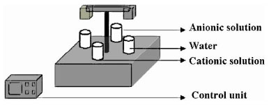 ) shows the sketch of SILAR set up used in this work. Dipping timings in the solution and distilled water can be varied from one to hundred seconds and number of SILAR cycles from one to five hundred. After five to ten cycles we replaced the rinsing water. This replacement of new water depends on the dipping timing in cationic and anionic precursors. The beakers containing solution and rinsing water are intercalated, each rinsing vessel being placed between a beaker containing solution of the salt of cation and the other containing solution of the salt of anion.
 |
Fig. (1) Sketch of the SILAR setup with control unit. |
Micro glass slides (6 cm x 1.25 cm) were cleaned thoroughly using soap solution to remove visible impurities and kept in chromic acid for 15 minutes. Later the slides were rinsed with distilled water. Two sets of Samples were prepared, one set using InCl3 and the other using In (NO3)3 as the cationic solution. The anionic precursor was Na2S solution for both the sets. Molar ratio between Indium and Sulfur was kept 1:1 for all the samples. Dipping time in precursor solution was varied from 2s to 15s in both cases. The samples were named in accordance with the dipping time as ‘AsBw’ where ‘A’ corresponds to dipping time in solution and ‘B’ the dipping time in water. Further the samples prepared using InCl3 were named ‘ICAsBw’ and those prepared using In(NO3)3 were named ‘INAsBw’.
Cleaned glass substrates were immersed for ‘n’ seconds in cationic precursor. This resulted in adsorption of Indium ions on to substrate surface. It was then immersed in distilled water for ‘n0’ seconds, in order to remove the de-adsorbed ions. These substrates were again immersed in for ‘n’ seconds in anionic precursor leading to adsorption and reaction of sulfide ions. Unreacted sulfide ions were removed by rinsing them in distilled water for ‘n0’ seconds. Thus a SILAR cycle is completed after these four operations. Repetition of SILAR cycle resulted in deposition of a thin layer of In2S3 on the substrate. These samples were annealed in vacuum at 1000C, 2000C, 3000C and 4000C for one hour [pressure ~ 10-5 Torr], in a chamber, made of glass tube over which Nichrome wire was wound uniformly along the entire length. This tube was heated by passing current through the Nichrome wire. Control of the temperature was achieved by adjusting the current. Four samples were placed in the vacuum chamber at a time. Temperature of sample was measured using chromel-alumel thermocouple, kept in contact with the samples. In all the cases, heating and cooling rate was 30C/minute.
Structural analysis was performed using x-ray diffraction (XRD) with a Rigaku (D.Max.C) x-ray diffractometer (CuKα (λ = 1.5405 Ao) radiation and Ni filter operated at 30 kV and 20 mA). Grain size of the films was calculated from the XRD pattern using Debye Scherrer’s formula, L=kλ/βcosθ, where L is the grain size, β is the full width half maximum of the peak (usually measured in radians). Optical absorption studies were carried out employing UV-VIS-NIR spectrophotometer (Hitachi model U-3410). Photosensitivity measurements were performed using Keithley 236 Source Measure Unit. The samples were illuminated with the help of a tungsten halogen lamp (white light) with intensity 60 mW cm-2. IR filter and water column were placed between the source and sample to avoid heating of the sample. The electric field applied to the film was 1000 V m-1. Silver electrodes were painted on the surface of the film on a fixed area with uniform thickness, keeping a distance of 5mm between the electrodes, for photosensitivity measurements. Photosensitivity is measured from the formula,
RESULTS AND DISCUSSION
Two sets of samples were prepared, one using InCl3 and sodium sulfide (Na2S) and other using In(NO3)3 and Na2S as precursor solutions. The dipping timings were varied from 2 to 15 seconds at room temperature. The number of SILAR cycles was kept 300 for all samples. When number of cycles was increased more than 300, film pealed off the substrate. Samples prepared using InCl3 and Na2S were yellow in color with good adhesion to the substrate; etching could be done with dilute hydrochloric acid. XRD pattern showed that all these samples were amorphous. It has been reported earlier that indium sulfide films prepared using InCl3 at room temperature through CBD and SILAR methods were also amorphous [16, 19, 20]. It was also reported that samples prepared using this method at deposition times 2s and 6s in precursor solution could be made crystalline upon annealing at 4000C [20]. Annealing temperature (Ta) is very important in the crystalline properties of the films.
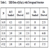
In the present work also samples prepared at 5s, 8s, 10s, 12s, 15s remained amorphous even after annealing at 1000C, 2000C and 3000C. But the sample annealed at 4000C showed crystalline nature having characteristic peaks of β-In2S3 with tetragonal structure (Fig. 2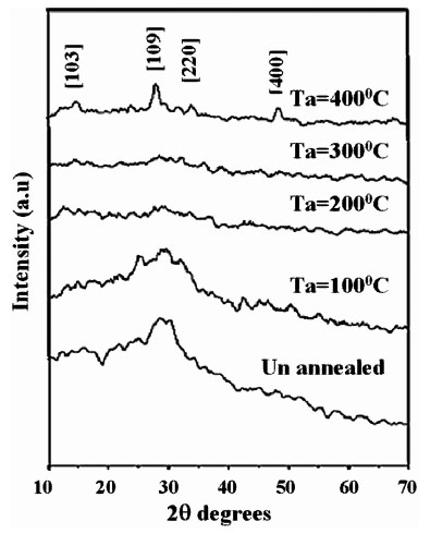 ). The d-values coincided with JCPDS file 25–390 as in Table 1. It is also clear from the XRD pattern that samples IC10s2w exhibited better crystalline nature compared to other samples (Fig. 3
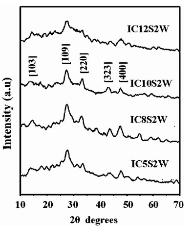 ). The sample IC2s10w having longer dipping time in water had poor crystallinity (Fig. 4
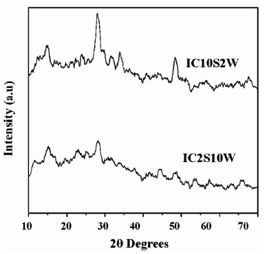 ). Grain size of these samples was calculated using Debye Scherer’s formula and this very well corroborated our observation that IC10s2w had better crystallinity. IC10s2w had grain size of 8.7 nm while IC2s10w films had grains of size 4.3 nm. However the grain size was found to increase with increase in dipping time in precursor solution (Fig. 3).
 |
Fig. (2) XRD Pattern of IC10s2w; pristine and annealed at 100°C, 200°C, 300°C, 400°C. |
 |
Fig. (3) XRD Pattern of IC5s2w, IC8s2w, IC10s2w, and IC12s2w annealed at 400°C. |
 |
Fig. (4) XRD pattern of IC10s2w and IC2s10w annealed at 400°C. |
The energy band gap calculated from the plot of (αhυ) 2vs hυ, [where ‘h’ is the Planck’s constant and ‘υ’ is the frequency], shows that all samples had direct band gap which slightly increase (from 2.26 eV to 2.54 eV) with decrease in dipping time in solution (from 15s to 5s). The sample IC10s2w had band gap of 2.32 eV while for IC2s10w band gap increases to 2.92 eV (Fig. 5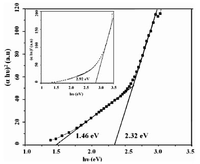 ). Optical band gap of β-In2S3 varies from 2.32 to 2.92 eV when the film was dipped in water for longer time (10s), which might be due to presence of oxygen. Barreau et al have reported similar results in the case of samples using CBD when the substrate is dipped for longer time in water [11]. XPS analysis on In2S3 films, prepared using SILAR, also suggests that films prepared with longer dipping time in water contains more oxygen [20]. During the film formation with longer dipping time in water, the grain growth is also affected leading to small grains and poor crystallinity. This may also lead to the wider band gap.
 |
Fig. (5) Band gap energy of pristine IC10s2w. (Inset: Energy band gap of pristine IC2s10w). |
Upon annealing at 4000C the band gap of samples (IC5s2w, IC8s2w, IC10s2w, IC12s2w and IC15s2w) reduced to 1.69 eV (Fig. 6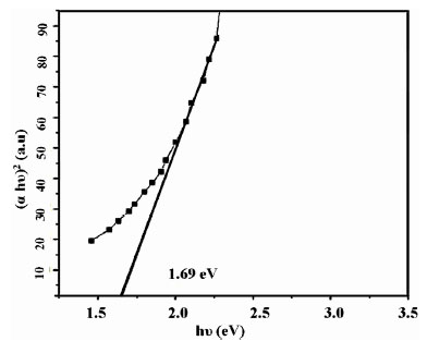 ). In the case of IC2s10w band gap reduces to 2.04 eV when annealed at 4000C. Vapor pressure of sulfur is very high and hence some sulfur may be escaping during annealing at 4000C. This might be one of the causes for reduction in bandgap on annealing. From Fig. (5), we find that apart from the band gap absorption at 2.32 eV there is a defect level absorption at 1.46 eV. But on annealing, this distinction between the two levels disappeared and the band gap reduces to 1.69 eV. This decrease in band gap upon annealing at 4000 C is attributed to the increase in the defect concentration below conduction band, which can be observed from the absorption spectra of both pristine and annealed samples [IC10s2w]. From Fig. (5) and Fig. (6), we observe that the absorbance for the annealed samples is much higher than the pristine due to the increase in defect concentration. This increase in absorbance for samples with better crystallinity might have been due to increase in oscillator strength.
 |
Fig. (6) Band gap energy of IC10s2w annealed at 400°C. |
All samples had low photoresponse with the photosensitivity varying from 0.3 to 2.0 and this increased upon annealing. Maximum photosensitivity of 2 was obtained for IC10s2w, which increased to 9.11 when annealed at 4000C. Probably the creation of more defect states below the conduction band upon annealing must be contributing to the increase in photoresponse. Number of SILAR cycles used for film fabrication was also found to affect film properties. At least 100 SILAR cycles were required for fabrication of uniform films. Below 100 cycles, the films were highly porous. The band gap decreased from 2.54 eV to 2.32 eV with increase in SILAR cycles from 100 to 300. The grain size increased with increase in SILAR cycles. But films deposited using 400 cycles were again porous. Hence we may conclude that for films fabricated using InCl3 and with 10s dipping time in solution and 2s in water, 300 SILAR cycles could give films of better properties in terms of band gap, crystallinity and photosensitivity.
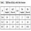
The films prepared using In (NO3)3 and Na2S were orange in color and were less adhesive to substrate. These films pealed off the substrate on annealing at temperature higher than 1000C. So studies on samples annealed at temperature higher than 1000C could not be done. The samples turned red on annealing, with the redness increasing as the annealing temperature increased. The pristine samples showed crystallinity with characteristic peaks corresponding to β-In2S3 with cubic structure and d- values coincided with JCPDS file 35 – 0456 (Table 2) [29]. Crystallinity improved up to 8s in solution and 2s in water (IN8s2w) and slowly reduces with increase in dipping time (Fig. 7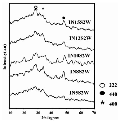 ). This is also evident from the grain size calculations since the grain size, which decreased with increase in dipping time in solution; grains were large (12.8 nm) for IN8s2w while it was 8.39 nm for IN10s2w and 5.02 nm for IN12s2w. But upon annealing at 1000C they showed poor crystallinity and grain size reduced to 8.2 nm for the sample IN10s2w. Being less adhesive to substrate, the grain size might have also diminished upon annealing as the films showed an increasing tendency to peel off the substrate with higher temperatures.
 |
Fig. (7) XRD Pattern of pristine samples prepared using In (NO3) 3. |
The band gap decreased from 2.05 eV to 1.93 eV on increasing the dipping time from 5s to 15s. Sample IN10s2w had band gap of 1.97 eV (Fig. 8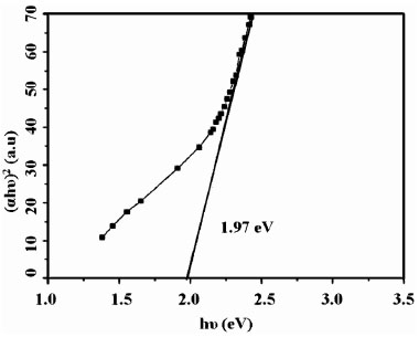 ). Annealing at 1000C, however, did not affect the band gap. IN10s2w had maximum photoresponse of 1.60 and annealing had no effect on photosensitivity in this case. Thus the photosensitivity of samples prepared using In (NO3)3 was lower than those, prepared using InCl3. The difference in photosensitivity of chloride and nitrate based In2S3 could also have been due to the difference in band gap. In the case of chloride based sample, before annealing, the band gap was comparable to that of nitrate based sample. In this case the photosensitivity was also comparable. But on annealing the band gap of chloride based samples decreased to 1.69 eV and thus resulted in higher absorption and higher photosensitivity. The increase in grain size for samples prepared with In (NO3)3 could be the reason why these samples are crystalline in the “as-prepared” condition. Hence SILAR appears to be a useful and easy way of deposition of buffer layers, as the required band gap and thickness can be controlled by merely varying the dipping times. Curbing the need for post deposition treatments for obtaining crystalline films by solely changing the precursor solution leaves us with opportunity to deposit of crystalline β-In2S3 buffer layer directly over the absorber layer of solar cells.
 |
Fig. (8) Band gap of pristine IN10s2w. |
CONCLUSION
Uniform, crystalline, cubic β-In2S3 with peak orientation along 440 plane could be fabricated using In(NO3)3 as precursor solution. The post deposition treatment (vacuum annealing at 4000C) which was required for obtaining crystalline β-In2S3 in the case of films using InCl3 as precursor can be curbed by using In (NO3)3. But films with good photo response were obtained only by annealing the chloride based samples at 4000C fabricated using InCl3. The optimum dipping time for obtaining crystalline films with good photosensitivity was 10s for chloride based samples and 8s for nitrate based samples. Thus SILAR is an easy method for fabricating films which can be used as buffer layers in solar cells.
ACKNOWLEDGEMENT
The authors would like to thank DST for funding through project and UGC for the financial support offered through DSA/COSIST schemes. One of the authors [ARW] is grateful to UGC for the fellowship. All authors are thankful to DST for some of the equipments used in this work were purchased with their financial support.