
The Open Materials Science Journal
(Discontinued)
ISSN: 1874-088X ― Volume 13, 2019
To Design a Cascode LNA by Using Channel-Length-Split Device with Constant-gm in a 0.35 μm Silicon CMOS Technology
Jui-Lin Lai*, Ting-You Lin, Cheng-Fang Tai, Rong-Jian Chen
Abstract
In the paper, the folded-cascode low-noise operational amplifier (LNA) with constant-gm is proposed and analyzed. The channel-length split technique adopted to expand ratio of W/L of the differential pair transistor to improve the performance of LNA for the gain bandwidth product, noise and offset voltage. The channel-length split method is separated differential input transistor into 2 transistors in series. The area of the transistor (W, L) can be properly increased to effectively decrease the flick noise. The double indirect-frequency compensation technique and the clamping circuit are adopted in amplifier to increase the bandwidth. The proposed two sets input differential pair can be provided a constant-gm value and rail-to-rail swing during the operating region. The floating-point structure is used to reach rail-to-rail swing at output stage. Simulation results show that the gain, constant-gm in input stag, noise, offset-voltage, PSRR, CMRR and ICMR of amplifier are improved. The characteristics of LNA are successfully verified by the TSMC 0.35um 2P4M CMOS technology. There have a great potential in the VLSI implementation used in the portable electronic and bio-medicine product applications.
Article Information

Identifiers and Pagination:
Year: 2016Volume: 10
Issue: Suppl-1, M8
First Page: 79
Last Page: 88
Publisher Id: TOMSJ-10-79
DOI: 10.2174/1874088X01610010079
Article History:
Received Date: 09/04/2015Revision Received Date: 15/05/2015
Acceptance Date: 08/07/2015
Electronic publication date: 15/07/2016
Collection year: 2016
open-access license: This is an open access article licensed under the terms of the Creative Commons Attribution-Non-Commercial 4.0 International Public License (CC BY-NC 4.0) (https://creativecommons.org/licenses/by-nc/4.0/legalcode), which permits unrestricted, non-commercial use, distribution and reproduction in any medium, provided the work is properly cited.
* Address correspondence to this author at the Department of Electronic Engineering, National United University, MiaoLi City 36003, Taiwan; E-mail: jllai@nuu.edu.tw
| Open Peer Review Details | |||
|---|---|---|---|
| Manuscript submitted on 09-04-2015 |
Original Manuscript | To Design a Cascode LNA by Using Channel-Length-Split Device with Constant-gm in a 0.35 μm Silicon CMOS Technology | |
INTRODUCTION
Recently, the low noise amplifier (LNA) is a one of important device in the analog circuit which is used in communication, high-frequency, and the required high-precision circuit applications. The various structure of amplifier is desired for difference propose in the dedicate applications. The amplifiers have gained preponderance over other linear amplifier for low power and low-voltage applications. Based on the gain and band-width of amplifier is a trade–off. The amplifier has a high-gain and high bandwidth performance is an important design issue. The other consideration is appropriately designed exhibit much higher power efficiency over a wide modulation index range with rail-to-rail signal swing [1Chang IK, Park JW, Kim SJ, Dal Kwack K. A global operational amplifier with constant-gm input and output stage. IEEE Region 10 Conf 1999; 2(15-17): 1051-4.-5Hong G-T, Shen C-H. A low offset high voltage swing rail-torailbuffer amplifier with for LCD driver. In: Proceedings IEEE Conferences
Electron Devices and Solid-State Circuits, EDSSC 2007.
[http://dx.doi.org/10.1109/EDSSC.2007.4450302] ]. The transconductance operational amplifier has constant-gm to increase the stability, but its band-width much poor [1Chang IK, Park JW, Kim SJ, Dal Kwack K. A global operational amplifier with constant-gm input and output stage. IEEE Region 10 Conf 1999; 2(15-17): 1051-4., 2Botma JH, Wassenaar RF, Wiegerink RJ. A low-voltage CMOS op amp with a rail-to-rail constant-gm input stage and a class ab rail-to-rail
output stage. In: IEEE International Symposium on Circuits and Systems, ISCAS'93 1993; pp. 1314-7.
[http://dx.doi.org/10.1109/ISCAS.1993.692895] ]. The class-AB amplifier with complementary differential input stage adopted offset cancellation to improve the offset voltage problem for the LCD driver [3Chih-Wen L. Amplifier with an offset cancellation for LCD drivers. IEEE J Solid-State Circ 2009; 44: 525-37.-5Hong G-T, Shen C-H. A low offset high voltage swing rail-torailbuffer amplifier with for LCD driver. In: Proceedings IEEE Conferences
Electron Devices and Solid-State Circuits, EDSSC 2007.
[http://dx.doi.org/10.1109/EDSSC.2007.4450302] ]. The Op-Amps has been compensated in Split-Length approach to process the frequency response compensation [6Jui-Lin L, Ting-You L, Cheng-Fang T, Yi-Te L, Rong-Jian C. Design a low-noise operational amplifier with constant-gm. In: Proceedings SICE. Taipei, Taiwan 2010; pp. 322-26. [August 18-21];-9Li Z, Sun L, Huang L. 0.4 mW wideband LNA with double gm enhancement and feed-forward noise cancellation. Electron Lett 2014; 50: 400-01.].
The common gate (CG) LNA uses double gm enhancement to provide input matching under low-power consumption. Feed-forward noise cancellation is employed in the LNA to suppress the noise from the CG transistor [9Li Z, Sun L, Huang L. 0.4 mW wideband LNA with double gm enhancement and feed-forward noise cancellation. Electron Lett 2014; 50: 400-01.].
Digital TV receiver should be capable of handling signals with broadband frequency that it is required that a wideband LNA should have sufficiently high gain and low noise figure (NF) to obtain the high sensitivity. When the operation frequency increases, common source (CS) configuration suffers from low-power (LP) gain that the multi-cascade stage is required. The cascode topology is adopted to overcome the large chip size for LNA design. It makes a compromise between the noise figure (NF) and the chip size. All reported techniques can reduce the NF, but they still require a high supply voltage in the multicascode topology. Circuit analysis and simulations validate the advantages of proposed topology to encounter design specifications [11Donggu I, Ilku N, Kwyro L. A CMOS active feedback balun-LNA with high IIP2 for wideband digital TV receivers. IEEE Trans Microwave Theory Tech 2010; 58(12): 3566-79.-14Mayank BT, Manoj A. Rajesh HK, Pravin AD. Multi-standard highly linear CMOS LNA. In: 2014 International Conference on Electronic Systems, Signal Processing and Computing Technologies. 2014; pp. 63-8.]. The organization of this paper is as follows. In first part, the compensation approaches for amplifier is presented. The structure of input stage with constant-gm is shown in the second part. The third part, the hardware structure of LNA in CMOS circuit’s realization is described. The simulations results are demonstrated and verified by HSPICE are shown in the fourth part. Finally, the conclusion is given.
CHANNEL-LENGTH SPLIT METHOD
The low-frequency noise is dominated from flick noise, is shown in the Fig. (1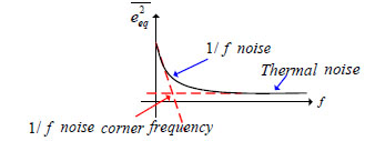 ). Noise voltage vn can be expressed by spectrum density in the equation (1) show that the second item is called flick noise can be effectively decreased by properly increasing the (W, L) geometry size of a transistor [10Baker RJ. CMOS Circuit Design, Layout, and Simulation. 2nd ed. Wiley-IEEE 2004. 978-0471700555].
 |
(1) |
 |
Fig. (1) Frequency spectrum for MOS noise voltage. |
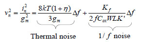
The totally capacitance is consist of inter-terminal, junction, line, and load capacitors for a MOS transistor at output node, that is Ctot = Cgd + Cdb + Cline + Cload. The transistor is adopted larger width to improve the noise and also make the frequency response become to poor. Using channel length split technique to reduce the gate-channel capacitance to reach the band-width improved.
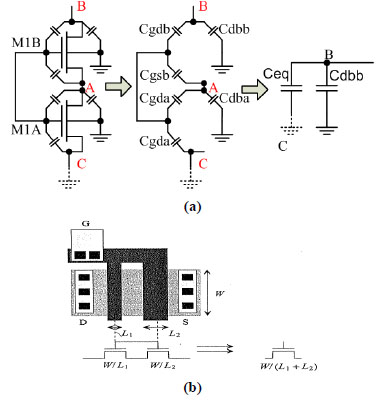 |
Fig. (2) Channel-length split (a) Equivalent model (b) Layout model. |
The channel-length split method is separated differential input transistor into 2 transistors in series, is shown in Fig. (2 ). The area of M1B transistor is designed to large then M1A to decrease the effect of flicks noise and increase the value of gm. In the really design, the transistor connected to output terminal is used the larger width. The equivalent circuits show that node A is floating-point and node C is virtual-ground. The equivalent capacitance Ceq from output node B is defined the serial path for Cgdb to Cgsa and Cgdb to Cdba. The equivalent capacitance changes to small base on the smaller capacitor Cgsa or Cdba in serial with the path. The channel-length split technique is reduced the total capacitance to improve the frequency response and take high gain. The split node is provided to use the indirect-compensation [6Jui-Lin L, Ting-You L, Cheng-Fang T, Yi-Te L, Rong-Jian C. Design a low-noise operational amplifier with constant-gm. In: Proceedings SICE. Taipei, Taiwan 2010; pp. 322-26. [August 18-21];-9Li Z, Sun L, Huang L. 0.4 mW wideband LNA with double gm enhancement and feed-forward noise cancellation. Electron Lett 2014; 50: 400-01.]. The channel-split used in PMOS and NMOS differential pairs are split to two transistors in serial that the node E and F to form low-impedance point is shown in Fig. (6
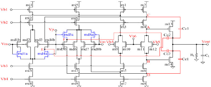 ). The output terminal feedback to those nodes is compensated by the miller capacitor. The amplifier applied the channel-split and the indirect compensation has the higher gain-bandwidth multiplication at low-noise.
INPUT-STAGE AND OUTPUT-STAGE
A. Input-Stage with Constant-gm
Base on take the good performance for input common mode range (ICMR) and wide-swing ability in the input stage of operational amplifier. The md1/md4 and md5/md8 are two set of PMOS and NMOS differential pair to improve the range of ICMR and wide-swing. The md2/md3 and md6/md7 are used to control the clamping circuit to limit the current of differential pair. Integrated both circuit to make a constant-gm circuit is shown in Fig. (3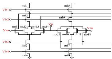 ). The operating mode of constant-gm circuit is respectively described for three regions as below.
 |
Fig. (3) Constant-gm circuit. |
Region I: when VCM, IVDD-2VSDP,SAT -VSGP, the differential pair (PMOS) is turn on and the other differential pair (NMOS) is lie in triode or turn-off region. Because gm2 is proportion to current that let Ii5 is equal to 4*Iref. Then the twice Irefis flow-through md5/md8, respectively. The totally gm expression is formulated during region I as (2).
Let β4= β5 =β and IDd4= IDd5 = I
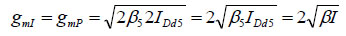 |
(2) |
Where gmI is express the transconductanc of differential pair for the region I.
Region II: When common mode voltage VCM,II>VSS+ 2VDSN,SAT+VGSN and VCM,IIVDD-2VSDP,SAT-VSGP. Because both PMOS and NMOS differential pair are turn on. Then the totally transconductance gm is rising up that is gmII = gmN + gmP. The clamping circuit md2/md3 and md6/md7 are used to limit its current. So that, the md1/md4 and md5/md8 flow-through current is limited at Iref/2 to induce the gmN and gmP are reduced. Its totally gm is expressed for region II as (3).
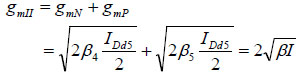 |
(3) |
Region III: When VCM,III>VSS+2VDSN,SAT+VGSN, the PMOS differential pair is lie in triode or turn-off region and the NMOS differential pair is turn on. The totally gm expression is formulated for region III as (4).
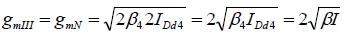 |
(4) |
The proposed differential pair can be provided a constant transconductance value during in the ranges for the operating region, where the values of gmI, gmII and gmIIIare equal to 2√βI. We can show that the performance of the two sets input differential pairs in the amplifier has a rail-to-rail and constant-gm for the input signal, is shown in the Fig. (4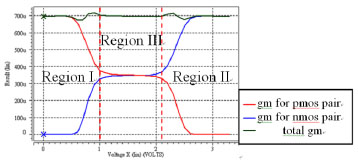 ).
).
 |
Fig. (4) Transconduction vs. input differential pair voltage. |
B. Floating Class AB Output-Stage
The operation of the traditional output amplifier is like as inverter that the transfer characteristic curve is expressed by the red line in the Fig. (5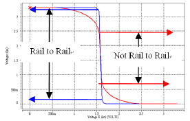 ). The result show that the curve has large slop related with the variation for the gate voltage of transistor to make the output swing can not reach rail-to-rail level. The proposed output stage is used the floating-potential structure in the class-AB amplifier to change the gate voltage of two transistors. The ratio of W/L in the transistor is properly tuning to adjust the variation of VDS. The transfer characteristic curve is expressedby the blue line in the Fig. (5). The simulation result show that the floating-potential and the properly ratio of W/L approaches can improve the amplifier to reach rail-to-rail output swing.
 |
Fig. (5) Transfer characteristic curve. |
LNA CMOS CIRCUIT REALIZATION
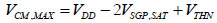
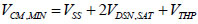
The folded-cascode operational amplifier with rail-to-rail, constant-gm input stage, and high-gain is shown in Fig. (6). The pre-stage is adopted folded-cascode circuit to produce full-swing and the output-stage is used class-AB push-pop amplifier. The amplifier used differential input structure with PMOS and NMOS in parallel be able to increase the range of ICMR value. The expression of the common mode voltage as (5) and (6)
 |
(5) |
 |
(6) |
 |
Fig. (6) The folded-cascode operational amplifier with capacitance cancellation. |
The MOS transistor pair md1a/md1b, md4a/md4b, md5a/md5b, and md8a/md8b are the differential structure with channel length split, where md1a, md4a, md5a, and md8a are operated in triode region. The transistors mi1, mi2, md2, md3, mi7, mi8, md6, and md7 construct the current clamping circuit. The differential pairs for PMOS and NMOS are acted by the used clamping circuit to limit the current flow and to reduce the transconductance of transistors. The output stage consisted by transistors m11~m14 is a class-AB push-pull amplifier with transconductance amplification properties. When the gate-source voltage (Vgs) in the m8 is changed, then the Vgs of m14 also follow changed by the current mirror pair. That is, the amplifier can translate input voltage variation into the related output current. The output node A and B is floating points in the LNA produce a feature for the output impedance independent to load. The load current is determined by the W/L ratio at output stage m13 and m14, power supply, and loads, is shown in Fig. (6).
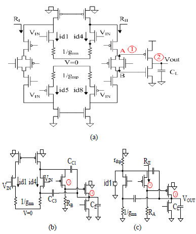 |
Fig. (7) (a) Small signal equivalent circuit for LNA. (b) Equivalent circuit for output of point A. (c) Equivalent circuit for (b). |
The small signal equivalent circuit of the proposed LNA is shown in Fig. (7a ). Assume point A is the output of 1-st stage. The concisely small signal equivalent circuits are shown in Fig. (7b, c). The small-signal analysis and the gain computing are based on the equivalent circuits.
 |
(7) |
 |
(8) |
 |
(9) |
 |
(10) |
The output resistance RA of the first stage is shown as below.
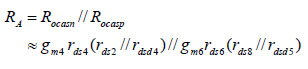 |
(11) |
 |
(12) |
 |
(13) |
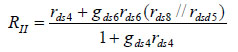
The small-signal model of the proposed LNA is shown in Fig. (8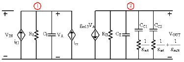 ). The RI (RII) and CI (CII)are expressed the equivalent impedance and capacitance from A (Vout) terminal of output stage, respectively. Two sets compensation capacitors are connected to point C, D, E, and F as shown in Fig. (6). The buffer current icc through compensation capacitor and transistor from output of amplifier feedback to the output point at 1-st amplifier. The buffer current icc is expressed in (14):
 |
Fig. (8) Small signal model. |
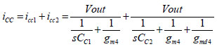 |
(14) |
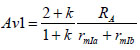
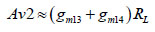
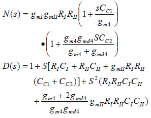
From the small signal model can find the transfer function is expressed as Vout(s)/Vin(s) = N(s)/D(s), where N(s) and D(S) are shown in as:
 |
(15) |
Let N(S) of transfer function equal to zero then the zero Z1 and Z2 of the system are solved as:
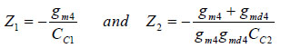 |
(16) |
Let D(S) of transfer function equal to zero then the pole P1 and P2 of the system are solved as:
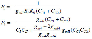 |
(17) |
To calculate the band-width of LNA at unit gain is:
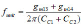 |
(18) |
SIMULATION RESULTS
To verify the validity of the proposed LNA, the amplifier is simulated by HSPICE for CMOS technology. We can show that the folded cascade amplifier have rail-to-rail and constant-gm properties for the input signal. As the simulation results, the open loop gain of amplifier is 98.8dB, band-width is 60MHz, and phase margin (PM) is 60° at 30pf load capacitance, are shown in Fig. (9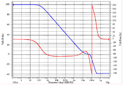 ). Noise and slew-rate analysis are shown in Fig. (10
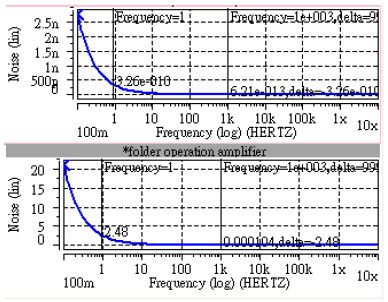 , 11
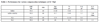
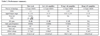
, 11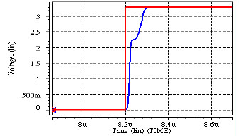 ), respectively. The performances for the different compensation methods are simulated are expressed in Table 1. Miller capacitor compensation is from output connect to points A and B. Miller with zero resistance compensation is from output connect to points A and B. Indirect compensation SL1 is from output connect to points A and B. Indirect compensation with channel separate SL2 is from output connects to points C, D, E, and F. The SL2 has a wide band-width and settle-time better than others. Detail the simulated data for the proposed LNA with SL2 compensation is summary in the Table 2. The performance of the proposed LNA is more batter than the published papers for the same CMOS technology.
 |
Fig. (9) Frequency response of LNA (BW=60MHz, PM=60°). |
 |
Fig. (10) Simulation for LNA noise. |
 |
Fig. (11) Simulation for LNA slew-rate. |
LNA is fabricated using the different MOS topologies that act as an amplifier along with the biasing circuitry. Therefore, the behaviors function of the proposed LNA is successfully verified by the TSMC 0.35μm 2P4M CMOS technology. The required die size for the desired chip is 1268μm×1176μm after layout, is shown in the Fig. (12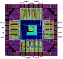 ). The power dissipation is estimated about 2.8mW.
 |
Fig. (12) Chip layout. |
CONCLUSION
The folded-cascade operational amplifier with rail-to-rail is realized in CMOS circuits, and verified by HSPICE for TSMC technology. The channel-length split approach applied to 2 PMOS and NMOS pairs into the differential pair of the proposed LNA can be obtained constant-gm in input stag, low-noise (24.92n) and low offset-voltage (25.78μV) properties. The amplifier with floating-potential and the properly ratio of W/L approaches to improve the rail-to-rail output swing. The double indirect-frequency compensation technique and the clamping circuit are adopted to increase the bandwidth. The proposed circuit has a high band-width (BW=60MHz), DC gain (98dB) and constant-gm for high stability, good sensitivity and distortion. The power supply rejection ratio (PSRR, 114.8 dB) and CMRR (137.8 dB) and input common mode range (ICMR) has been improved. The proposed LNA is successfully implemented by the TSMC 0.35μm 2P4M silicon CMOS technology. The required die size for the desired chip is a 1268μm×1176μm layout area.
CONFLICT OF INTEREST
The authors confirm that this article content has no conflict of interest.
ACKNOWLEDGEMENTS
In this work, authors would like to thank was supported by the Ministry of Science & Technology of Taiwan, ROC to carry out research work. The National Chip Implementation Center (CIC) and Taiwan Semiconductor Manufacturing Corporation (TSMC) provide some support and auxiliary for 0.35μm CMOS technology.
REFERENCES
| [1] | Chang IK, Park JW, Kim SJ, Dal Kwack K. A global operational amplifier with constant-gm input and output stage. IEEE Region 10 Conf 1999; 2(15-17): 1051-4. |
| [2] | Botma JH, Wassenaar RF, Wiegerink RJ. A low-voltage CMOS op amp with a rail-to-rail constant-gm input stage and a class ab rail-to-rail
output stage. In: IEEE International Symposium on Circuits and Systems, ISCAS'93 1993; pp. 1314-7. [http://dx.doi.org/10.1109/ISCAS.1993.692895] |
| [3] | Chih-Wen L. Amplifier with an offset cancellation for LCD drivers. IEEE J Solid-State Circ 2009; 44: 525-37. |
| [4] | Weng M-C, Wu J-C. A compact low-power rail-to-rail class-B buffer for LCD column driver. IEICE Trans Electron 2002; E85-C(8): 1659-63. |
| [5] | Hong G-T, Shen C-H. A low offset high voltage swing rail-torailbuffer amplifier with for LCD driver. In: Proceedings IEEE Conferences
Electron Devices and Solid-State Circuits, EDSSC 2007. [http://dx.doi.org/10.1109/EDSSC.2007.4450302] |
| [6] | Jui-Lin L, Ting-You L, Cheng-Fang T, Yi-Te L, Rong-Jian C. Design a low-noise operational amplifier with constant-gm. In: Proceedings SICE. Taipei, Taiwan 2010; pp. 322-26. [August 18-21]; |
| [7] | Saxena V, Baker RJ. Indirect feedback compensation of CMOS op-amps. In: IEEE/EDS Workshop on Microelectronics and Electron Devices (WMED). 2006; pp. 3-4. |
| [8] | Saxena V, Baker RJ. Compensation of CMOS op-amps using split-length transistors. In: Proceedings of the 51st Midwest Symposium on
Circuits and Systems. 2008; pp. 109-2. [http://dx.doi.org/10.1109/MWSCAS.2008.4616748] |
| [9] | Li Z, Sun L, Huang L. 0.4 mW wideband LNA with double gm enhancement and feed-forward noise cancellation. Electron Lett 2014; 50: 400-01. |
| [10] | Baker RJ. CMOS Circuit Design, Layout, and Simulation. 2nd ed. Wiley-IEEE 2004. 978-0471700555 |
| [11] | Donggu I, Ilku N, Kwyro L. A CMOS active feedback balun-LNA with high IIP2 for wideband digital TV receivers. IEEE Trans Microwave Theory Tech 2010; 58(12): 3566-79. |
| [12] | Yeh H-C, Chiong C-C, Aloui S, Wang H. Analysis and design of millimeter-wave low-voltage CMOS cascode LNA With magnetic coupled technique. IEEE Trans Microwave Theory Tech 2012; 60(1): 4066-79. |
| [13] | Khurram Muhammad, R S M. A 3–5 GHz current-reuse -boosted CG LNA for ultrawideband in 130 nm CMOS. IEEE Trans Very Large Scale Integr Syst 2012; 20(3): 400-9. |
| [14] | Mayank BT, Manoj A. Rajesh HK, Pravin AD. Multi-standard highly linear CMOS LNA. In: 2014 International Conference on Electronic Systems, Signal Processing and Computing Technologies. 2014; pp. 63-8. |