- Home
- About Journals
-
Information for Authors/ReviewersEditorial Policies
Publication Fee
Publication Cycle - Process Flowchart
Online Manuscript Submission and Tracking System
Publishing Ethics and Rectitude
Authorship
Author Benefits
Reviewer Guidelines
Guest Editor Guidelines
Peer Review Workflow
Quick Track Option
Copyediting Services
Bentham Open Membership
Bentham Open Advisory Board
Archiving Policies
Fabricating and Stating False Information
Post Publication Discussions and Corrections
Editorial Management
Advertise With Us
Funding Agencies
Rate List
Kudos
General FAQs
Special Fee Waivers and Discounts
- Contact
- Help
- About Us
- Search


The Open Electrical & Electronic Engineering Journal
(Discontinued)
ISSN: 1874-1290 ― Volume 13, 2019
Multilayer Neural Network with Synapse Based on Two Successive Memristors
Minh-Huan Vo*
Abstract
Introduction:
Synapse based on two successive memristors builds the synaptic weights of the artificial neural network for training three-bit parity problem and five-character recognition.
Methods:
The proposed memristor synapse circuit creates positive weights in the range [0;1], and maps it to range [-1;1] to program both the positive and negative weights. The proposed scheme achieves the same accuracy rate as the conventional bridge synapse schemes which consist of four memristors.
Results and Conclusion:
However, proposed synapse circuit decreases 50% the number of memristors and 76.88% power consumption compared to the conventional bridge memristor synapse.
Article Information

Identifiers and Pagination:
Year: 2018Volume: 12
First Page: 132
Last Page: 147
Publisher Id: TOEEJ-12-132
DOI: 10.2174/1874129001812010132
Article History:
Received Date: 8/10/2018Revision Received Date: 25/11/2018
Acceptance Date: 11/12/2018
Electronic publication date: 31/12/2018
Collection year: 2018
open-access license: This is an open access article distributed under the terms of the Creative Commons Attribution 4.0 International Public License (CC-BY 4.0), a copy of which is available at: https://creativecommons.org/licenses/by/4.0/legalcode. This license permits unrestricted use, distribution, and reproduction in any medium, provided the original author and source are credited.
* Address correspondence to this author at the Department of Electrical and Electronics Engineering, Ho Chi Minh University of Technology and Education, 01 Vo Van Ngan, Thu Duc District, Ho Chi Minh City, Vietnam; Tel: 909437522; E-mail: huanvm@hcmute.edu.vn
| Open Peer Review Details | |||
|---|---|---|---|
| Manuscript submitted on 8-10-2018 |
Original Manuscript | Multilayer Neural Network with Synapse Based on Two Successive Memristors | |
1. INTRODUCTION
An artificial neural network is a mathematical model which was built based on biological neural networks. It consists of a group of artificial neurons connected together, and handles information by transmitting links and calculating new values at the nodes [1L.O. Chua, and L. Yang, "Cellular neural networks: Theory", IEEE Trans. Circ. Syst., vol. 35, no. 10, pp. 1257-1272.
[http://dx.doi.org/10.1109/31.7600] , 2L.O. Chua, and L. Yang, "Cellular neural networks: Applications", IEEE Trans. Circ. Syst., vol. CAS-35, no. 10, pp. 1273-1290.
[http://dx.doi.org/10.1109/31.7601] ]. In fact, many neural networks are non-linear statistical data modeling tools. They can be used to model complex relationships between input data and output results or to search for patterns in data. This study of artificial neural network is one of the sectors concerned so much in recent years. The neural network chips require energy efficiency and small size to be able to design a model with hundreds, thousands of neurological nodes. Currently, these nodes are often designed with CMOS components, but gradually the transistor size is not scaled according to the uptrend number of CMOS in one chip every year. This is because it is limited in its physics characteristics [3L.O. Chua, "Memristor – the missing circuit element", IEEE Trans. Circuit Theory, vol. 18, no. 5, pp. 507-519.
[http://dx.doi.org/10.1109/TCT.1971.1083337] ]. Originally, synapses were developed by CMOS circuits. However, each synapse requires too much power and area.
The memristor (memory resistor) was invented by Chua in 1971 as the fourth basic element of electrical circuits [3L.O. Chua, "Memristor – the missing circuit element", IEEE Trans. Circuit Theory, vol. 18, no. 5, pp. 507-519.
[http://dx.doi.org/10.1109/TCT.1971.1083337] ]. This device has a special ability to change its resistance when a current or voltage is applied to the terminals. When the current or voltage is stopped, this device still holds the state at that moment without loss for a long time. Memristor has been extensively studied in compatibility with CMOS as a nonvolatile memory or logic gate to improve production technology with a fast speed chip, power-saving, low cost, simple structure and denser integrated level. Especially, the memory resistors are used as synapses to mimic the functions of a real brain [4M. Chu, "Neuromorphic hardware system for visual pattern recognition with memristor array and CMOS neuron", IEEE Trans. Ind. Electron., vol. 62, no. 4, pp. 2410-2419.
[http://dx.doi.org/10.1109/TIE.2014.2356439] ]. Memristor is much smaller in size compared to the previous CMOS technology. In 2008, Stanley Williams and his group realized memristor in the form of a device in laboratory practice HP [5D.B. Strukov, G.S. Snider, D.R. Stewart, and R.S. Williams, "The missing memristor found", Nature, vol. 453, no. 7191, pp. 80-83.
[http://dx.doi.org/10.1038/nature06932] [PMID: 18451858] ].
Innate property of reconfigurable resistor allows memristor as being highly suitable for designing synapse weights [6P.M. Sheridan, C. Du, and W.D. Lu, "Feature extraction using memristor networks", IEEE Trans. Neural Netw. Learn. Syst., vol. 27, no. 11, pp. 2327-2336.
[http://dx.doi.org/10.1109/TNNLS.2015.2482220] [PMID: 26513807] -9A. M. Sheri, H. Hwang, M. Jeon, and B-G Lee, "Neuromorphic character recognition system with two pcmo memristors as a synapse", IEEE Trans Indus Electron, vol. 61, no. 6, .]. The hybrid CMOS-Memristor architectures have been presented for synaptic connections due to the compatibility characteristics between CMOS technology and Memristor [8I. Vourkas, and G. Ch. Sirakoulis, "Emerging memristor-based logic circuit design approaches: A review", IEEE Circuits Syst. Mag., vol. 16, no. 3, pp. 15-30.
[http://dx.doi.org/10.1109/MCAS.2016.2583673] -11S. Sayyaparaju, S. Amer, and G.S. Rose, "A bi-memristor synapse with spike-timing-dependent plasticity for on-chip learning in memristive neuromorphic systems", 19th Int Sympo Quality Electron Design (ISQED), .
[http://dx.doi.org/10.1109/ISQED.2018.8357267] ]. Most previous implementations of memristor based learning rules have focused on Spike-Timing Dependent Plasticity (STDP) [10C. Zamarreño-Ramos, L.A. Camuñas-Mesa, J.A. Pérez-Carrasco, T. Masquelier, T. Serrano-Gotarredona, and B. Linares-Barranco, "On spike-timing-dependent-plasticity, memristive devices, and building a self-learning visual cortex", Front. Neurosci., vol. 5, p. 26.
[http://dx.doi.org/10.3389/fnins.2011.00026] [PMID: 21442012] -13R. Legenstein, C. Naeger, and W. Maass, "What can a neuron learn with spike-timing-dependent plasticity?", Neural Comput., vol. 17, no. 11, pp. 2337-2382.
[http://dx.doi.org/10.1162/0899766054796888] [PMID: 16156932] ]. The energy efficient STDP is seriously restricted by the lack the effective learning algorithms. The architecture of synapse with 1Transtistor and 1 memristor has been proposed recently with the help of a weight-dependent STDP learning rule [11S. Sayyaparaju, S. Amer, and G.S. Rose, "A bi-memristor synapse with spike-timing-dependent plasticity for on-chip learning in memristive neuromorphic systems", 19th Int Sympo Quality Electron Design (ISQED), .
[http://dx.doi.org/10.1109/ISQED.2018.8357267] ]. However, it causes the area overhead and power loss to conduct learning tasks. The STDP learning rules are suitable for single-layer neural network with a few inputs per neuron. Moreover, the convergence of STDP based learning is not guaranteed for general inputs [13R. Legenstein, C. Naeger, and W. Maass, "What can a neuron learn with spike-timing-dependent plasticity?", Neural Comput., vol. 17, no. 11, pp. 2337-2382.
[http://dx.doi.org/10.1162/0899766054796888] [PMID: 16156932] ].
To reduce the circuit size, the memristor-based crossbar array architecture is presented with fewer memristors and transistors. Here, both positive polarity and minus-polarity connection matrices are realized by a single crossbar and a simple constant-term circuit, thus, reducing the physical size and power dissipation [14S.N. Truong, and K-S. Min, "New memristor-based crossbar array architecture with 50-% area reduction and 48-% power saving for matrixvector multiplication of analog neuromorphic computing", J. Semicond. Tech. Sci., vol. 14, no. 3, pp. 356-363.
[http://dx.doi.org/10.5573/JSTS.2014.14.3.356] ]. However, it is limited to a single layer neural network in fundamental processing tasks. Therefore, the multilayer neural network is proposed to extend the single layer network to a higher dimension complex tasks of multiprocessing.
Recently, it has been highlighted that a memristor array design can be used to train single-layer neural network on very large datasets with perceptron algorithm [15F. Alibart, E. Zamanidoost, and D.B. Strukov, "Pattern classification by memristive crossbar circuits using ex situ and in situ training", Nat. Commun., vol. 4, p. 2072.
[http://dx.doi.org/10.1038/ncomms3072] [PMID: 23797631] ]. However, general multilayer neuron network cannot be trained with perceptron algorithm. The scalable training of Multiplayer neuron network requires the back-propagation algorithm. Specially, it can achieve good results on large dataset. Multilayer neural network and back-propagation algorithm have proved a powerful learning scheme to implement neuronmorphic system efficiently with hardware [16S.P. Adhikari, "A circuit-based learning architecture for multilayer neural networks with memristor bridge synapses", IEEE Trans. Circ. Syst., vol. 62, no. 1, pp. 215-223.-19Y. Zhang, X. Wang, and E.G. Friedman, "Memristor-based circuit design for multilayer neural networks", IEEE Trans. Circ. Syst., vol. 65, pp. 677-686.].
So far, there has been no circuit to implement online learning on MNNs. On-chip learning methods remain a challenge in most memristor based synapses. Recently, the artificial synapse, consisting of multiple identical memristors that are arranged in a bridge-like architecture is a promising candidate for circuit based on back propagation learning architecture for neural networks [16S.P. Adhikari, "A circuit-based learning architecture for multilayer neural networks with memristor bridge synapses", IEEE Trans. Circ. Syst., vol. 62, no. 1, pp. 215-223., 17H. Kim, M.P. Sah, C. Yang, T. Roska, and L.O. Chua, "Neural synaptic weighting with a pulse-based memristor circuit", IEEE Trans. Circuits Syst. I, Reg. Papers, vol. 59, no. 1, pp. 148-158.]. Here, learning method implemented on-chip using memristor bridge synapse was proposed [16S.P. Adhikari, "A circuit-based learning architecture for multilayer neural networks with memristor bridge synapses", IEEE Trans. Circ. Syst., vol. 62, no. 1, pp. 215-223., 17H. Kim, M.P. Sah, C. Yang, T. Roska, and L.O. Chua, "Neural synaptic weighting with a pulse-based memristor circuit", IEEE Trans. Circuits Syst. I, Reg. Papers, vol. 59, no. 1, pp. 148-158.]. By using the bridge memristor synapse circuit, it can create both positive and negative weighting values that are easy to implement neuromorphic system in hardware. Thus, the weight of each synapse will be changed by applying a specific pulse width. It is noted that the weighting has to be programed linearly according to pulse width. As the result, the artificial synapse can be behaved in reality. The main challenge for this synaptic circuit arises from the power consumption and area which are contained in a multiplicative term and is hard to implement in compact hardware. Recent solutions have been published for memristor based neuromorphic systems. Memristor based multiplayer with online gradient descent training was proposed using single memristor and two CMOS transistor per a synapse [18D. Soudry, D. Di Castro, A. Gal, A. Kolodny, and S. Kvatinsky, "Memristor-based multilayer neural networks with online gradient descent training", IEEE Trans. Neural Netw. Learn. Syst., vol. 26, no. 10, pp. 2408-2421.
[http://dx.doi.org/10.1109/TNNLS.2014.2383395] [PMID: 25594981] ]. A memristor based single-layer neural network is expanded into a multiplayer neural network [19Y. Zhang, X. Wang, and E.G. Friedman, "Memristor-based circuit design for multilayer neural networks", IEEE Trans. Circ. Syst., vol. 65, pp. 677-686.]. A memristor based AND logic switch is utilized to update synaptic crossbar circuit which requires area and power overhead and nonlinear characteristics of programming memristor.
In this paper, we propose a synapse circuit structure by using advanced memristor architecture. Every synapse consists of two successive memristors and no transistor as compared to the conventional memristors described in [16S.P. Adhikari, "A circuit-based learning architecture for multilayer neural networks with memristor bridge synapses", IEEE Trans. Circ. Syst., vol. 62, no. 1, pp. 215-223.-19Y. Zhang, X. Wang, and E.G. Friedman, "Memristor-based circuit design for multilayer neural networks", IEEE Trans. Circ. Syst., vol. 65, pp. 677-686.]. The synapse weighting model is updated lineally according to pulse width. An adaptive back-propagation algorithm for the proposed multilayer neural network is used to train neural network and perform the parity checker and character recognition. Thus, our proposed synapse is reduced by a half the number of memristors. We use two kinds of square pulse. Here, a pulse with large width is used to program the synaptic weights and a pulse with small width is used to compute the weight and input.
2. MEMRISTOR AND SYNAPTIC WEIGHT CIRCUIT
2.1. Memristor Model
In 2008, Stanley Williams and his group realized memristor in the form of a device in laboratory HP. To create memristor, they used a thin titanium oxide film (TiO2) [5D.B. Strukov, G.S. Snider, D.R. Stewart, and R.S. Williams, "The missing memristor found", Nature, vol. 453, no. 7191, pp. 80-83.
[http://dx.doi.org/10.1038/nature06932] [PMID: 18451858] ]. The film is connected with 2 poles made of platinum (Pt). One pole is injected with oxygen holes. These oxygen holes are positively charged ions. Therefore, there is a transition layer of TiO2 with a mixed side and one side is not mixed.
Let us define the thickness of the doped region w, D is the thickness of two layers TiO2 and RON, ROFF are low and high impedance respectively. Accordingly, the memristance M(t) of the TiO2 memristor model is given by equation (1)
 |
(1) |
Where  is the state variable of memristor.
The relationship between the voltage v(t) and current i(t) of the memristor is given in equation (2)
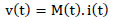 |
(2) |
State variables x(t) are determined:
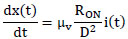 |
(3) |
Where µv is the dopant mobility. Velocity of the width change is linearly proportional to the current as in equation (3). Thus, we call this model linear model.
Various types of nonlinear memristor model have been published. One of them is in the window model in which the state equation is multiplied by window function Fp(w), namely in equation (4)
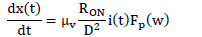 |
(4) |
Where p is a parameter and Fp(w) is defined by: in equation (5)
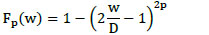 |
(5) |
This is called the nonlinear drift model. It means that as the p decreases, the nonlinearity increases. In other words, as the p increases, the model tends to the linear one as shown in Fig. (1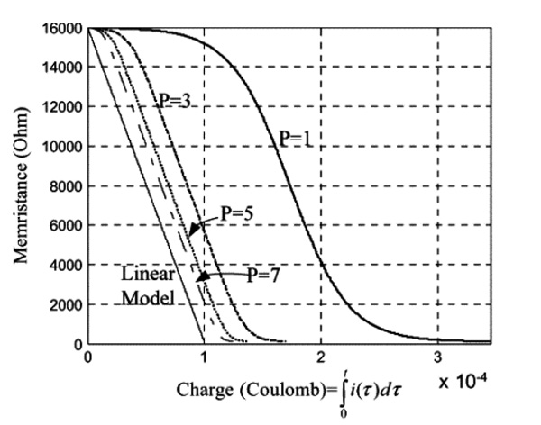 ).
).
 |
Fig. (1) Memristance of memristor with p parameter. |
2.2. Synapse Circuit Based on Two Successive Memristors
The conventional memristor bridge synapse operates like a Wheatstone bridge consisting of four identical memristors with the polarities indicated in Fig. (2a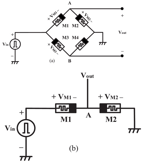 ) [10C. Zamarreño-Ramos, L.A. Camuñas-Mesa, J.A. Pérez-Carrasco, T. Masquelier, T. Serrano-Gotarredona, and B. Linares-Barranco, "On spike-timing-dependent-plasticity, memristive devices, and building a self-learning visual cortex", Front. Neurosci., vol. 5, p. 26.
[http://dx.doi.org/10.3389/fnins.2011.00026] [PMID: 21442012] ]. The input signal is applied from the left side of the circuit and the output is taken from two middle nodes as a differential form. When strong pulse Vin is applied at the input, the memristance of each memristor is increased or decreased depending upon its polarity. For instance, when a positive pulse is applied as an input, the memristances of M1 and M4 whose polarities are forward biased will decrease. On the other hand, the memristances of M2 and M3 whose polarities are reverse biased, will increase. It follows that the voltage VA at node A with respect to the ground becomes smaller than the voltage VB at node B. Since, the node voltage VA is less than VB, the output voltage Vout across the bridge is negative weight. Memristor bridge circuit linearly generates synaptic weights in the range [-1;1] [10C. Zamarreño-Ramos, L.A. Camuñas-Mesa, J.A. Pérez-Carrasco, T. Masquelier, T. Serrano-Gotarredona, and B. Linares-Barranco, "On spike-timing-dependent-plasticity, memristive devices, and building a self-learning visual cortex", Front. Neurosci., vol. 5, p. 26.
[http://dx.doi.org/10.3389/fnins.2011.00026] [PMID: 21442012] ].
 |
Fig. (2) (a) Memristor bridge circuit [10C. Zamarreño-Ramos, L.A. Camuñas-Mesa, J.A. Pérez-Carrasco, T. Masquelier, T. Serrano-Gotarredona, and B. Linares-Barranco, "On spike-timing-dependent-plasticity, memristive devices, and building a self-learning visual cortex", Front. Neurosci., vol. 5, p. 26. [http://dx.doi.org/10.3389/fnins.2011.00026] [PMID: 21442012] ].(b)The proposed scheme of synapse based on two successive memristors. |
Two successive memristors are similar to half-bridge circuit consisting of two memristors shown in Fig. (2b). When we want to get positive or negative value, strong pulse Vin is applied at the input, the memristance of each memristor is increased or decreased depending upon its polarity. For instance, when a positive pulse is applied as an input, the memristances of M1 decrease. On the other hand, the memristances of M2 increase. Because the circuit acts as a half-bridge, we can only program positive weights in the range [0;1].
If Vin is input signal applied to the memristor haft-bridge circuit in Fig. (2b) at time t, the input voltage will be divided by the well-known “voltage – divider formula” as follows: in eq 6 and equation 7
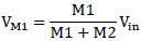 |
(6) |
 |
(7) |
Where M1, and M2 denote the corresponding memristances of the memristors at time t, in Fig. (2b).
The output voltage Vout of the circuit is equal to the voltage at terminal A, namely in equation 8
 |
(8) |
From (8), the voltage Vout is given in equation 9,
 |
(9) |
Where  represents the synaptic weight of the successive memristor circuit.
The successive memristor circuit could only generate positive weights in the range [0;1] corresponding to each weight of memristor circuit. Thus, we have to map weights from the range [0;1] to range [-1;1] so that we can program the synapse weighting.
Fig. (3a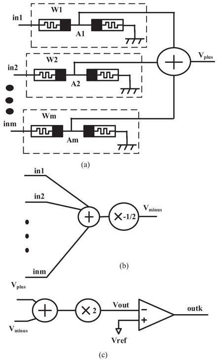 ) describes a perceptron network with m inputs and m synapses. We have the following equation: (10)

 |
(10) |
Conventionally, weights of w1, w2, ..., wm covering in [-1,1] are used to set synapse weighting in bridge memristor synapse [10C. Zamarreño-Ramos, L.A. Camuñas-Mesa, J.A. Pérez-Carrasco, T. Masquelier, T. Serrano-Gotarredona, and B. Linares-Barranco, "On spike-timing-dependent-plasticity, memristive devices, and building a self-learning visual cortex", Front. Neurosci., vol. 5, p. 26.
[http://dx.doi.org/10.3389/fnins.2011.00026] [PMID: 21442012] ]. The input signals are from in1 to inm. Y is an output summation of the perceptron network. However, the circuit of two successive memristors only creates weighting in range [0;1] as explained in equation (8). To transfer the weights w1, w2, ..., wm from the range [-1;1] to the new range [0;1], this weight is divided by 2, then adding 0.5. For instance, If the w1 is -1 weighting in range [-1;1], the new w1 weighting will be 0 in range [0,1]. In other hand, If w1 weighting is 1, the new w1 weighting will be 1 in range [0;1].
From (10), after transferring weights to the new range [0;1], we have the following equation: (11)
 |
(11) |
Where, Z is new output when in range [0;1].
From (11), we have the following equation: (12)
 |
(12) |
From (10) and (12), we get this equation: (13)
 |
(13) |
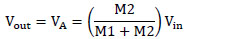
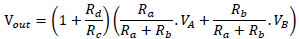
We can see the formula (13) shown in Fig. (3c). Where, Z is Vplus, A is Vminus and Y is Vout.
In Fig. (3a), the positive weights are installed in the range [0;1]. In Fig. (3b), negative values are created to compensate weightings in the range [-1;1]. In Fig. (3c), we sum positive and negative values and double the result to achieve Vout . Then Vout is compared with Vref to determine output of outk with k corresponding to the number of output neurons in equation (14).
 |
(14) |
3. SIMULATION RESULTS
Our successive memristor architecture is simulated using HP TiO2 memristor model. The basic parameters for the simulations are based on the data given by HP, where RON=100Ω, ROFF=16 KΩ, qmax = 6e-5 C.
In the weight setting, a pulse with long width is applied to change the state of memristor and a narrow pulse for synaptic multiplication is applied to avoid the drifting the memristor state. The weight setting of the architecture is verified through computer simulations and synaptic multiplication. Memristor synapse based neural circuit is performed by Cadence tool.
In the weight setting, a pulse with long width of 1V amplitude is applied to change the state of memristor. Fig. (4a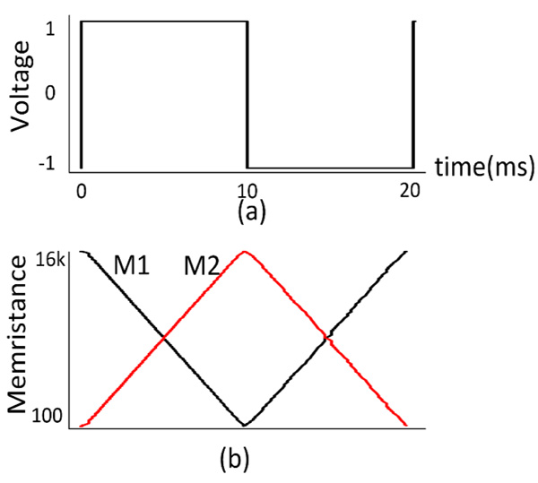 ) shows square pulse inputs with an amplitude +1V. Fig. (4b) shows the memristance changes of M1(t) and M2(t) according to a time function for a positive and negative pulse, obtained via simulations of the successive memristor circuit in Fig. (4) with initial memristances; M1(0) = 16 KΩ, M2(0) = 100 Ω. We start to set the memristance of M1 that is 16 Kohm and M2 that is 100 Ohm. Because the polarity of M1 is opposite to M2, the memristance of M1 will be decreased and the memristance of M2 will be increased when applying a positive pulse. Otherwise, when applying a negative pulse, the memristance of M1 will be increased and the memristance of M2 will be decreased. From that, to set initial weight, we apply a pulse with the width based on time duration. However, if we apply too long pulse, the weight will get 0 or 1, and if we apply too short pulse, the weight will not be changed. From this, we can use a short pulse as an input pulse to implement the multiplication between the input and the weight. The weight
  will increase if applying positive pulse and will decrease if applying a negative pulse.
 |
Fig. (4) Variation of memristance and voltages, when positive and negative pulses are applied to the memristor synapse (a) Positive and negative input voltage pulses; (b) Memristance variations. |
As shown in the Fig. (4b), these numerically computed memristances and the corresponding weight are very linear according to various times.
3.1. Training on Hardware with 3-bit Parity Problem
The parity function is used very often in digital systems for error detection and correction. Parity system is also used to detect hardware failures in digital memory. The digital additions and multiplications also require parity circuits. The parity circuit is usually implemented by cascading XOR gates. This solution for N-bit parity requires N-1 XOR gates. Thus, this circuit consists of several layers and introduces significant delays. The modular neural networks are suitable to solve these parity problems [11S. Sayyaparaju, S. Amer, and G.S. Rose, "A bi-memristor synapse with spike-timing-dependent plasticity for on-chip learning in memristive neuromorphic systems", 19th Int Sympo Quality Electron Design (ISQED), .
[http://dx.doi.org/10.1109/ISQED.2018.8357267] ].
Fig. (5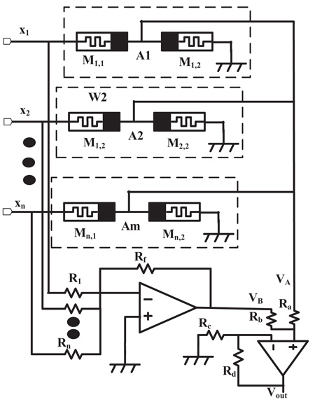 ) shows a detail implementation circuit of two successive memristor architecture. A set of x1,...,xn plays a role as inputs of neural network system. A two successive memristor array represents a weight array of Ψ1,...,Ψn. A negative amplifier with n inputs are connected to n resistors. To get value -½ as expected, we have: in equation 15
 |
(15) |
if we assume that  , we can obtain in equation (16)
 |
(16) |
Next, a multiplier of 2 with two inputs is presented. The output of Vout is calculated by in equation 17
 |
(17) |
With 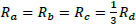 ,
,
 |
(18) |
 |
Fig. (5) Detail circuit of successive memristor architecture. |
Fig. (6 ) shows the neural network model of training 3-bit parity. The 3-bit parity is trained by a neural network with three inputs, six neurons in hidden layer and one output. The weights of hidden layer are a set of
  and the weights of output layer are a set of
  . Beside, the biases are added in each neuron in hidden layer and output layer. The biases of hidden layer are a set of
  and the bias of the output layer is b2. The input is in the range of [-1; 1] and the output is in the range of [-1; 1].
 |
Fig. (6) The neural network model to train 3-bit parity problem with three inputs, six neurons in hidden layer and one output. |
Table 1 shows the truth table of 3-bit parity problem and the encoding used for input bits and output bits for implementations to satisfy the weight programming process. The odd parity problem counts the number of bit 1s to determine the output value. If the number of bit 1s is odd, the output bit will be 1. If the number of bit 1s is even, the output bit will be 0. The bit 0 will be encoded to -1, the bit 1 will be encoded to 1.

Fig. (7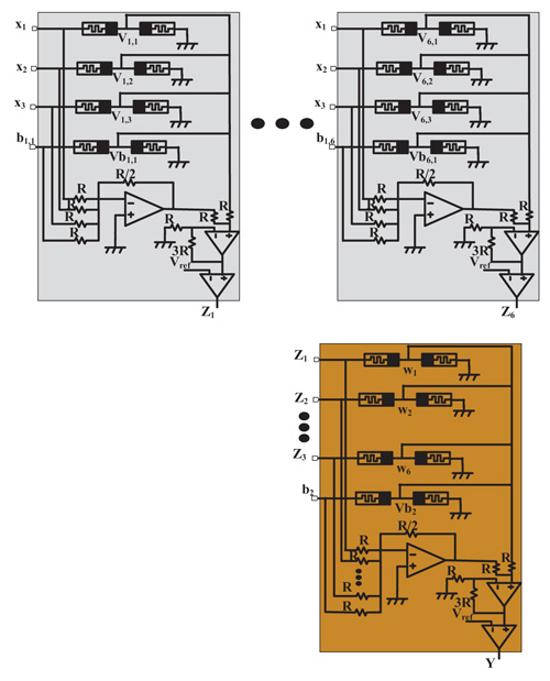 ) shows detail connections of 3-bit parity training circuit. Each neuron in the hidden layer is performed by each column in the circuit. It includes 4 pairs of memristors consisting of 3 weights of
  and 1 weight of bias input. For example, the first column has 3 pairs of memristors that are
  and fourth pair is vb1,1. The output of the first column is Z1. Similarly, the outputs of other six columns are a set from Z1 to Z6. After that, all neurons in hidden layer are connected to the output neuron. It is performed by orange column. It includes 7 pairs of memristors that are 6 weights of the output layer from w1 to w6 and one weight of the input bias as vb2. A comparison circuit with reference voltage is added to generate the output in range [-1; 1] as Table 1. All resistor values are explained in equations from 15 to 18.
 |
Fig. (7) Detail connection of the 3-bit parity circuit. |
The Back-propagation algorithm is utilized to updating memristance. The training algorithm based on the back-propagation is stated as:
- Set random weight for each pair of memristors.
- For each input x:
- Apply input to determine hidden layer and output values.
- Calculate error between the neuron output and desired output: d-y.
- Update weights of output layer and hidden layer.
- If the error is not covered, go to step 2, else, finish training.
 |
(19) |
 |
(20) |
The operations in the training process for the neural network can be broken into three major steps as the following:
- Apply inputs to hidden layer and output layer to determine neuron errors.
- Back-propagate the errors through the output layer weights and hidden layer weights.
- Update the synaptic weights for both layers of neurons.
Step 1: A set of inputs is applied to the hidden layer, and the output layer is measured. Then, the algorithm determines the difference between neuron output and the desired output. These values are generated using a comparator that provides a discretized error value of +1 or -1. Thus, these errors can easily be recorded in binary form for later use.
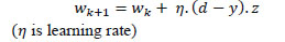
Step 2: The errors are applied to the output layer weights and hidden layer weights as Eq. 19 and Eq. 20
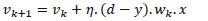
Step 3: To update weight, based on the pulse difference between reference pulse and input pulse, we get plus pulse width modulation circuit as shown in waveform of Fig. (8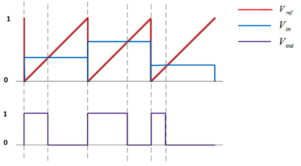 ). As known, the memristance is changed when applying positive pulse or negative pulse. Because memristor can store its state, we just need to update ∆w or ∆v instead of wk+1 or vk+1 as shown in Fig. (9
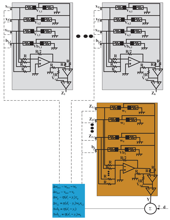 ).
).
 |
Fig. (8) Waveform shows different pulse widths for different input magnitude. Vout shows pulse width of modulation circuit output. |
 |
Fig. (9) Circuit model of the neural network. |
Fig. (10 ) shows the training curve obtained from simulations of MATLAB – CADENCE SPECTRE utilizing the back-propagation algorithm. After nine epochs, the error approaches to zero, it means that the training process was successful.
 |
Fig (10) Learning curve for three bit input parity problem. |
3.2. Image Recognition
Fig. (11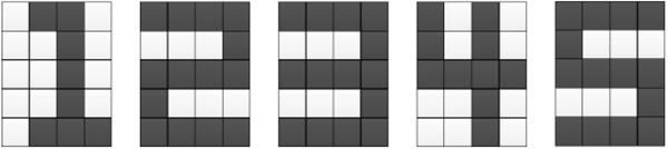 ) shows the prototype of the five digits. Each digit has 10 samples and is put into training process. The more the sample, the higher the training accuracy. Here we only train 10 samples with each digit. To increase the precision of the actual recognition application, the more samples should be put into training.
 |
Fig. (11) Training images. |
Each sample in Fig. (11) is a 5x4 sized character and each weight will be programmed by synaptic circuit including two successive memristors. Thus, we design 20 memristor synaptic circuits for 20 synapse weights.
Fig. (12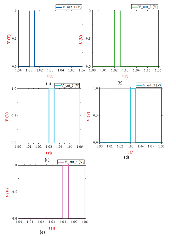 ) shows the results of simulation output voltage of each digit from 1 to 5. The results show that we can identify the output digit based on the output voltage level. Among five output voltages, the digit can be recognized by setting a threshold voltage level. For instance, when we use digit 1 recognition circuit that we will take the result as in Fig. (12a). The output voltage is 1 V if input is digit 1 and output is 0 if the inputs are the other digits such as 2, 3, 4 or 5. Similarly, the output voltage of digit-2 recognition circuit is 1V as in Fig. (12b) if input is digit 2, else output voltage is 0V in the other digit inputs. Figs. (12c, d, e) is corresponding to digit 3, digit 4, and digit 5, respectively.
 |
Fig. (12) Output simulation results for 5 digits with synapse based on two successive memristors. |
Fig. (13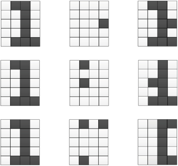 ) describes the character in interference noise. We take digit-1 character as an example. The percentage of noise is shown in this figure. Noise ratio is calculated by noise bits over a total data bits. For example, a noisy bit is added to a 5 x 4 size sample, we achieve a noise rate of 5%. Table 2 shows the recognition rate when the interference noise is occurring. Recognition accuracy will greatly reduce according to the number of the added noise bit.
 |
Fig. (13) Noisy patterns added for recognition test at 5%, 10%, and 15%. |
Table 2 shows the successful identification rate for 5 digits. The results show the same identification rate among the two circuit schemes. There is no difference in recognition rate between the two schemes. When noise patterns increase, the recognition rate will greatly decrease. For example, the digit 1 gets 100% successful identification rate with no noise effect in both the conventional memristor bridge circuit and the proposed successive memristor circuit. At 15% added noise patterns, the recognition rate of 60% is achieved for both techniques of memristor bridge circuit and successive memristor circuit. However, the successive memristor circuit will save half the number of memristors. The CMOS transistors in the proposed technique are also less than in the memristor bridge circuit. Thus, area and power consumption of the proposed circuit will be smaller for the conventional memristor bridge circuit.

The system consists of five recognition circuits in parallel; each circuit corresponds to a digit from 1 to 5. The conventional identification circuit uses synapses that are conducted by bridge memristor circuits. Each circuit includes 20 synapses. Each synapse uses 4 memristors. Thus, the system uses 400 memristors in all 5 identification circuits for digits from 1 to 5. The number of CMOS transistor is 62 for each identification circuit. The system consists of 5 circuits consuming 310 CMOS transistors as shown in Table 3.

The proposed identification circuit uses 20 synapses that are constructed from two successive memristors. The proposed system has all 5 circuits, so total memristors are 200. We have a total of 140 CMOS corresponding to 5 proposed recognition circuits for 5 digits from 1 to 5 as shown in Table 3.
Thus, the synaptic circuit using two successive memristors occupies a smaller area than the conventional memristor bridge synapse circuit.
Fig. (14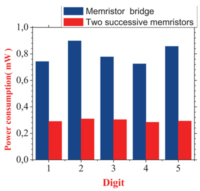 ) and Table 4 show clearly that the synapse of the two-successive memristors consumes less than the conventional memristor bridge synapse circuit in terms of power dissipation. The proposed technique can save upto 76.88% power loss compared to the conventional memristor bridge circuit in case of No.5 digit recognition. This is because the area of the proposed successive memristor circuit is designed with smaller numbers of memristor and CMOS transistor compared to the conventional memristor bridge circuit. Here, the accuracy recognition rate is the same among two techniques.
 |
Fig. (14) Power consumption in the two character identification circuits for each digit. |

CONCLUSION
In this paper, we proposed a synaptic circuit which is able to perform signed synaptic weighting. Synaptic weights are trained with hardware. The recognition rates achieve 100% success for digits from 1 through 5. Each digit has 10 samples and each sample is formed in a 5x4 matrix. The 5%, 10%, and 15% noisy patterns are added to consider the recognition rate. The results of the character recognition rate show that successive memristor circuit is equivalent to the conventional memristor bridge circuit, but it is a smaller haft than in term of overhead area. The proposed memristor synapse saves up to 76.88% power consumption compared to the conventional bridge memrsitor synapse circuit.
CONSENT FOR PUBLICATION
Not applicable.
CONFLICT OF INTEREST
The authors declare no conflict of interest, financial or otherwise.
ACKNOWLEDGEMENTS
Decleared none.
REFERENCES
| [1] | L.O. Chua, and L. Yang, "Cellular neural networks: Theory", IEEE Trans. Circ. Syst., vol. 35, no. 10, pp. 1257-1272. [http://dx.doi.org/10.1109/31.7600] |
| [2] | L.O. Chua, and L. Yang, "Cellular neural networks: Applications", IEEE Trans. Circ. Syst., vol. CAS-35, no. 10, pp. 1273-1290. [http://dx.doi.org/10.1109/31.7601] |
| [3] | L.O. Chua, "Memristor – the missing circuit element", IEEE Trans. Circuit Theory, vol. 18, no. 5, pp. 507-519. [http://dx.doi.org/10.1109/TCT.1971.1083337] |
| [4] | M. Chu, "Neuromorphic hardware system for visual pattern recognition with memristor array and CMOS neuron", IEEE Trans. Ind. Electron., vol. 62, no. 4, pp. 2410-2419. [http://dx.doi.org/10.1109/TIE.2014.2356439] |
| [5] | D.B. Strukov, G.S. Snider, D.R. Stewart, and R.S. Williams, "The missing memristor found", Nature, vol. 453, no. 7191, pp. 80-83. [http://dx.doi.org/10.1038/nature06932] [PMID: 18451858] |
| [6] | P.M. Sheridan, C. Du, and W.D. Lu, "Feature extraction using memristor networks", IEEE Trans. Neural Netw. Learn. Syst., vol. 27, no. 11, pp. 2327-2336. [http://dx.doi.org/10.1109/TNNLS.2015.2482220] [PMID: 26513807] |
| [7] | J. Zhang, X. Wang, and Eby G. Friedman, "Memristor-based circuit design for multilayer neural networks", IEEE Trans. Circuits Systems, vol. 65, no. 2, pp. 677-686. |
| [8] | I. Vourkas, and G. Ch. Sirakoulis, "Emerging memristor-based logic circuit design approaches: A review", IEEE Circuits Syst. Mag., vol. 16, no. 3, pp. 15-30. [http://dx.doi.org/10.1109/MCAS.2016.2583673] |
| [9] | A. M. Sheri, H. Hwang, M. Jeon, and B-G Lee, "Neuromorphic character recognition system with two pcmo memristors as a synapse", IEEE Trans Indus Electron, vol. 61, no. 6, . |
| [10] | C. Zamarreño-Ramos, L.A. Camuñas-Mesa, J.A. Pérez-Carrasco, T. Masquelier, T. Serrano-Gotarredona, and B. Linares-Barranco, "On spike-timing-dependent-plasticity, memristive devices, and building a self-learning visual cortex", Front. Neurosci., vol. 5, p. 26. [http://dx.doi.org/10.3389/fnins.2011.00026] [PMID: 21442012] |
| [11] | S. Sayyaparaju, S. Amer, and G.S. Rose, "A bi-memristor synapse with spike-timing-dependent plasticity for on-chip learning in memristive neuromorphic systems", 19th Int Sympo Quality Electron Design (ISQED), . [http://dx.doi.org/10.1109/ISQED.2018.8357267] |
| [12] | N. Zheng, and P. Mazumder, "Learning in memristor crossbar-based spiking neural networks through modulation of weight-dependent spike-timing-dependent plasticity", IEEE Trans. Nanotech, vol. 17, no. 3, . |
| [13] | R. Legenstein, C. Naeger, and W. Maass, "What can a neuron learn with spike-timing-dependent plasticity?", Neural Comput., vol. 17, no. 11, pp. 2337-2382. [http://dx.doi.org/10.1162/0899766054796888] [PMID: 16156932] |
| [14] | S.N. Truong, and K-S. Min, "New memristor-based crossbar array architecture with 50-% area reduction and 48-% power saving for matrixvector multiplication of analog neuromorphic computing", J. Semicond. Tech. Sci., vol. 14, no. 3, pp. 356-363. [http://dx.doi.org/10.5573/JSTS.2014.14.3.356] |
| [15] | F. Alibart, E. Zamanidoost, and D.B. Strukov, "Pattern classification by memristive crossbar circuits using ex situ and in situ training", Nat. Commun., vol. 4, p. 2072. [http://dx.doi.org/10.1038/ncomms3072] [PMID: 23797631] |
| [16] | S.P. Adhikari, "A circuit-based learning architecture for multilayer neural networks with memristor bridge synapses", IEEE Trans. Circ. Syst., vol. 62, no. 1, pp. 215-223. |
| [17] | H. Kim, M.P. Sah, C. Yang, T. Roska, and L.O. Chua, "Neural synaptic weighting with a pulse-based memristor circuit", IEEE Trans. Circuits Syst. I, Reg. Papers, vol. 59, no. 1, pp. 148-158. |
| [18] | D. Soudry, D. Di Castro, A. Gal, A. Kolodny, and S. Kvatinsky, "Memristor-based multilayer neural networks with online gradient descent training", IEEE Trans. Neural Netw. Learn. Syst., vol. 26, no. 10, pp. 2408-2421. [http://dx.doi.org/10.1109/TNNLS.2014.2383395] [PMID: 25594981] |
| [19] | Y. Zhang, X. Wang, and E.G. Friedman, "Memristor-based circuit design for multilayer neural networks", IEEE Trans. Circ. Syst., vol. 65, pp. 677-686. |
| [20] | B.M. Wilamowski, D. Hunter, and A. Malinowski, "Solving parity-N problems with feedforward neural networks", Proc. Int. Jt. Conf. Neural Netw., vol. 4, pp. 2546-2551. |